

A kind of fast green environmental protection double-sided polishing method of silicon wafer substrate
A green and double-sided polishing technology, which is applied in the manufacture of electrical components, circuits, semiconductors/solid-state devices, etc., can solve the problems of low polishing process time cost, difficulty in conforming to the epitaxial process, increasing substrate stress, etc., to shorten the processing time , rapid polishing, and the effect of reducing surface defects and damage
- Summary
- Abstract
- Description
- Claims
- Application Information
AI Technical Summary
Problems solved by technology
Method used
Image

Examples
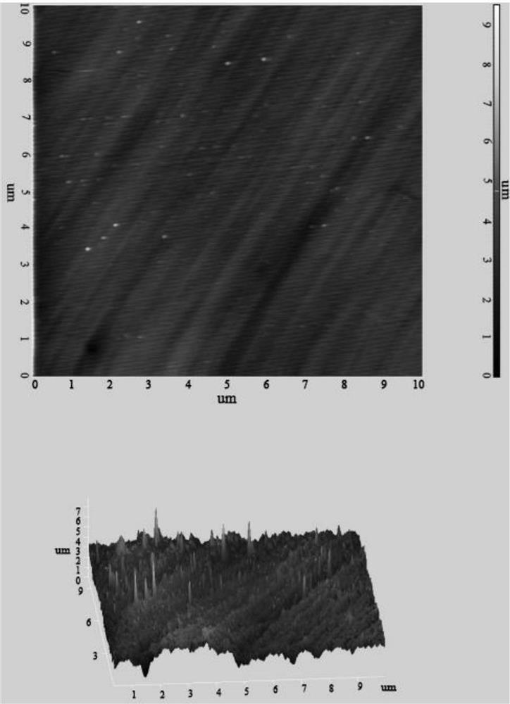
Embodiment 1
[0027] A kind of fast green environmental protection double-side polishing method of silicon wafer substrate, comprises the following steps:
[0028] (1) Loading: Take five 4-inch silicon wafer substrates and place them in the star wheel;
[0029] (2) Rough polishing: the silicon wafer substrate is chemically mechanically polished with a rough polishing solution, and after polishing, it is ultrasonically cleaned with deionized water and ethanol for 10 min, and dried; the rough polishing solution is composed of cerium oxide, deionized water, Prepared from dispersant and pH adjusting agent;
[0030] (3) Fine polishing: the silicon wafer substrate is chemically mechanically polished with a fine polishing solution after rough polishing, ultrasonically cleaned with deionized water and ethanol for 10 minutes respectively after polishing, and dried; the fine polishing solution is composed of cerium oxide, deionized Prepared with ionized water and dispersant.
[0031] In the present...
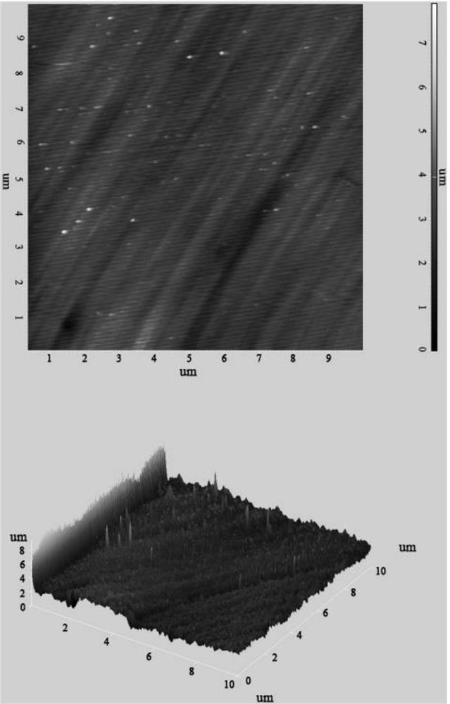
Embodiment 2
[0035] A kind of fast green environmental protection double-side polishing method of silicon wafer substrate, comprises the following steps:
[0036] (1) Loading: Take five 4-inch silicon wafer substrates and place them in the star wheel;
[0037] (2) Rough polishing: the silicon wafer substrate is chemically mechanically polished with a rough polishing solution, and after polishing, it is ultrasonically cleaned with deionized water and ethanol for 10 min, and dried; the rough polishing solution is composed of cerium oxide, deionized water, Prepared from dispersant and pH adjusting agent;
[0038] (3) Fine polishing: the silicon wafer substrate is chemically mechanically polished with a fine polishing solution after rough polishing, ultrasonically cleaned with deionized water and ethanol for 10 minutes respectively after polishing, and dried; the fine polishing solution is composed of cerium oxide, deionized Prepared with ionized water and dispersant.
[0039] In the present...
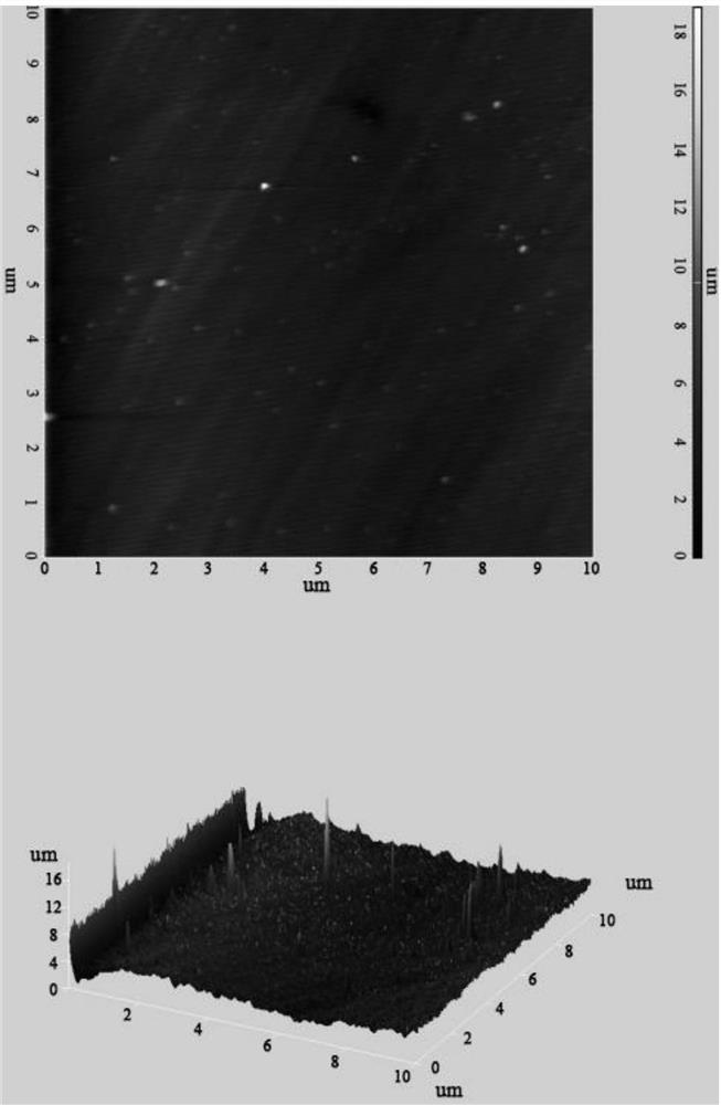
Embodiment 3
[0043] A kind of fast green environmental protection double-side polishing method of silicon wafer substrate, comprises the following steps:
[0044] (1) Loading: Take five 4-inch silicon wafer substrates and place them in the star wheel;
[0045] (2) Rough polishing: the silicon wafer substrate is chemically mechanically polished with a rough polishing solution, and after polishing, it is ultrasonically cleaned with deionized water and ethanol for 10 min, and dried; the rough polishing solution is composed of cerium oxide, deionized water, Prepared from dispersant and pH adjusting agent;
[0046](3) Fine polishing: the silicon wafer substrate is chemically mechanically polished with a fine polishing solution after rough polishing, ultrasonically cleaned with deionized water and ethanol for 10 minutes respectively after polishing, and dried; the fine polishing solution is composed of cerium oxide, deionized Prepared with ionized water and dispersant.
[0047] In the present ...
PUM
| Property | Measurement | Unit |
|---|---|---|
| particle diameter | aaaaa | aaaaa |
| particle diameter | aaaaa | aaaaa |
| surface roughness | aaaaa | aaaaa |
Abstract
Description
Claims
Application Information