Device for polishing outer peripheral edge of semiconductor wafer

a technology for peripheral edges and polishing machines, which is applied in the direction of edge grinding machines, lapping machines, manufacturing tools, etc., can solve the problems of inefficient polishing process and difficult to obtain highly precise polishing, and achieve stable polishing efficiency, coarse polishing surface, and high polishing efficiency.

Inactive Publication Date: 2005-07-26
ISHII HYOKI
View PDF4 Cites 23 Cited by
  • Summary
  • Abstract
  • Description
  • Claims
  • Application Information

AI Technical Summary

Benefits of technology

[0004]In light of the above, it is an object of the present invention to provide a polishing machine for a peripheral edge of a semiconductor wafer, capable of highly precise, uniform, highly efficient, and stable polishing.
[0007]Since according to the present invention, contactless polishing is conducted by drawing polishing solution into the gap between the peripheral edge of semiconductor wafer and the rotary body, the peripheral edge of semiconductor wafer can be polished in a highly precise and uniform manner. Additionally, because the polishing pad of existing methods is not needed, polishing pad changing and adjustments are not necessary, allowing for a stable polishing process.
[0009]Additionally, in the above-mentioned construction, a dynamic pressure generating grooves can be formed on the peripheral surface of the rotary body, facing the periphery of the semiconductor wafer. Because, according to this construction, the flow speed of polishing solution is increased through the dynamic pressure effect of the dynamic pressure generating grooves, the polishing efficiency is increased.
[0010]Additionally, in the above-mentioned construction, a magnet may be installed in the rotary body, and a magnetic polishing solution may be used as the polishing solution. Because, according to this construction, the magnetic polishing solution is confined by the magnet of the rotary body, the polishing efficiency is increased.
[0012]In the polishing machine of the present invention, the polishing efficiency and coarseness of the polished surface are influenced by such factors as polishing speed (the relative rotating speed of the semiconductor wafer and the rotary body), the flow speed and pressure of polishing solution in the above-mentioned gaps, the viscosity of the polishing solution, and the concentration and diameter of abrasive particles in the polishing solution. However, by forming at least the peripheral surface of the rotary body from an elastic material with a hardness of 7-40 Hs, variations in the values of the above-mentioned factors are absorbed by the appropriate elasticity of the rotary body peripheral surface, making it possible to constantly obtain a stable polishing efficiency and level of polished surface coarseness. Additionally, during the polishing process, the polishing speed may be changed (for example, polishing with a relatively high polishing speed for a prescribed length of time from the start of the polishing process, then polishing at a relatively lower polishing speed for the remainder of the polishing process) without changing the semiconductor wafer holding status, the polishing solution, or the like, enabling highly precise, highly efficient polishing.

Problems solved by technology

Chamfering processes of the peripheral edge of semiconductor wafers have had the following problems, due to the fact that the chamfering radius is small and the chamfering corners are steeply inclined: even with a flexible polishing pad it is unfeasible to obtain uniform contact with the surface of the peripheral edge, making it difficult to obtain highly precise polishing, and because only a small part of the surface of the pad is in contact with the edge surface, for instance a point or a line, the polishing process is inefficient.

Method used


Image

  • Device for polishing outer peripheral edge of semiconductor wafer
  • Device for polishing outer peripheral edge of semiconductor wafer
  • Device for polishing outer peripheral edge of semiconductor wafer

Examples


first embodiment

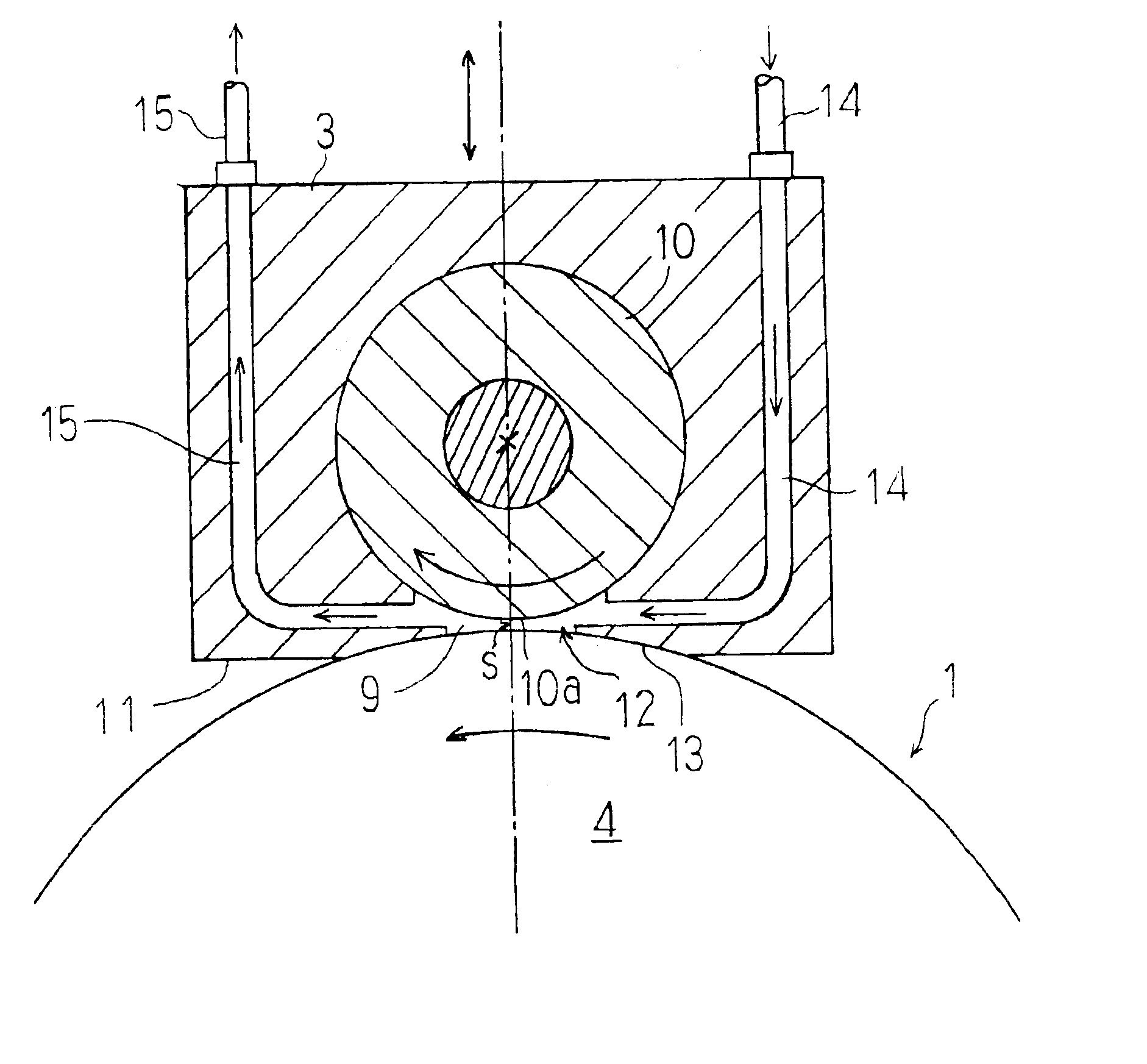
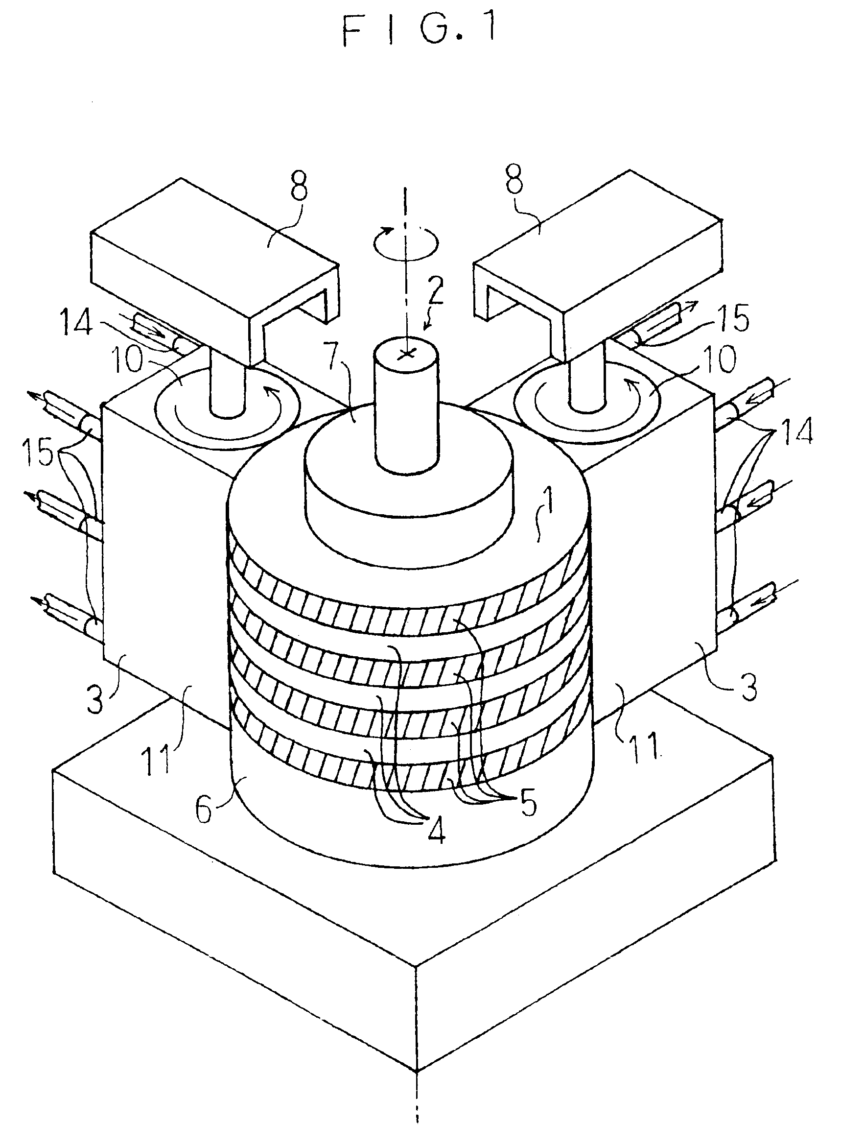
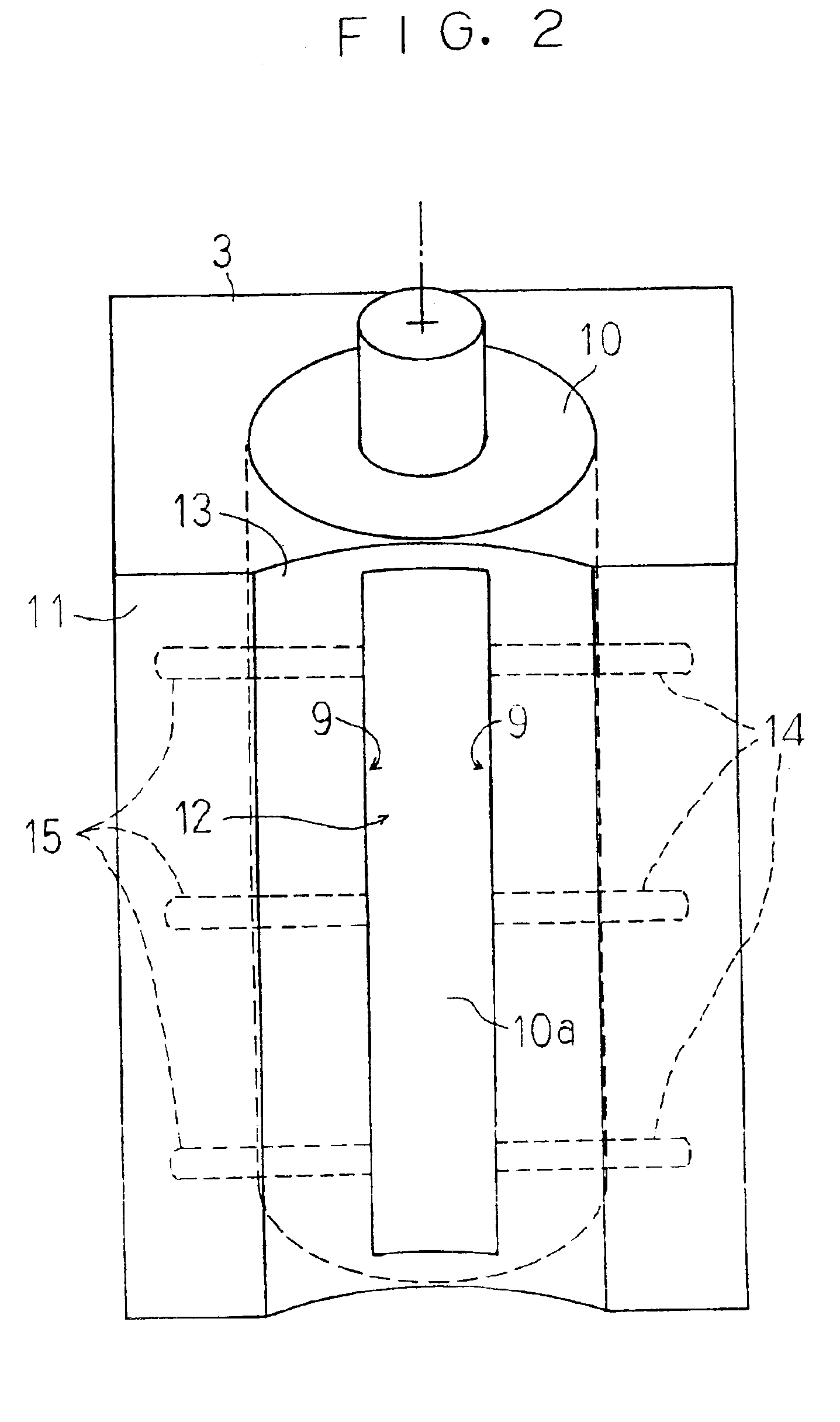
[0022]As shown in FIG. 1, the polishing machine for a peripheral edge of a semiconductor wafer according to the present invention comprises a rotary mechanism 2 on which is mounted and rotated a stack 1 of semiconductor wafers 4, and a polishing mechanism 3 which can be moved as desired along the radial direction of the rotary mechanism 2, and which polishes the peripheral edges of the rotating semiconductor wafers 4 via a contactless polishing process.

[0023]The peripheral edges of semiconductor wafers 4, having for example the shapes of circular plates, are chamfered as necessary, and notches (omitted from the drawing) are formed on the periphery at prescribed locations. The stack 1 of the semiconductor wafers 4 is aligned with the notches, and formed by placing spacers 5 between each semiconductor wafer 4. Note that the stack 1 of semiconductor wafers 4 is preferably provided with spacers 5 on the top and the bottom thereof, in order to keep from marking the surface of the wafers ...

second embodiment

[0035]Next, a polishing machine for a peripheral edge of a semiconductor wafer according to the present invention will be described.

[0036]As shown in FIG. 5, the polishing machine for a peripheral edge of a semiconductor wafer according to this embodiment is made up of the entire polishing machine for a peripheral edge of the first embodiment, immersed in a polishing solution tank 21 filled with polishing solution.

[0037]The polishing solution tank 21 is equipped with a polishing solution circulation apparatus 25. The polishing solution circulation apparatus 25 has two communicating pipes: a supply pipe 22 installed in the upper portion of the polishing solution tank 21, and a drain pipe 23 installed in the lower portion thereof, and circulates polishing solution in and out of the polishing solution tank 21. The polishing solution is collected from the lower portion of the polishing solution tank 21 by the polishing solution circulation apparatus 25, and after its temperature is regu...

third embodiment

[0043]Next, a polishing machine for a peripheral edge of a semiconductor wafer according to the present invention will be described.

[0044]As shown in FIG. 6, in this polishing machine for a peripheral edge, a rotary mechanism 2 upon which is mounted a stack 1 of semiconductor wafers 4, and an interior pipe body 32 mounted on the periphery of the stack 1 of semiconductor wafers 4, are accommodated inside an approximately cylindrical exterior pipe body 31 installed on the base thereof. Polishing solution is drawn into the minute gap between the stack 1 of semiconductor wafers 4 and interior pipe body 32, polishing the peripheral edges of the semiconductor wafers 4.

[0045]As in the first embodiment, the rotary mechanism 2 is equipped with a turntable 6 upon which is mounted the stack 1 of semiconductor wafers 4, and a locking piece 7 which presses the stack 1 of semiconductor wafers 4 onto the turntable 6, and fixes it thereto.

[0046]The exterior pipe body 31 serving as a polishing solut...


PUM

PropertyMeasurementUnit
dynamic pressureaaaaaaaaaa
hardnessaaaaaaaaaa
circumferenceaaaaaaaaaa

Abstract

A polishing machine for a peripheral edge of a semiconductor wafer comprises a rotary mechanism 2 which rotates a stack 1 of semiconductor wafers 4 mounted thereon, and a polishing mechanism 3 which is arranged to be movable in the radial direction of the rotary mechanism 2 and polishes the peripheral edges of the rotating semiconductor wafers 4 by means of contactless polishing. Minute gaps s are formed between the rotary column 10 of the polishing mechanism 3 and the stack 1 of semiconductor wafers 4, and polishing solution is drawn into these minute gaps s. The peripheral edges of the semiconductor wafers 4 are polished by means of contactless polishing, using polishing abrasive particles included in polishing solution.

Description

BACKGROUND OF THE INVENTION[0001]The present invention relates to a polishing machine for polishing the peripheral edge of a semiconductor wafer.[0002]The peripheral edges of semiconductor wafers made from silicon and the like are chamfered, but in recent years, further polishing of the peripheral edge has come to be conducted in order to prevent particle formation on the peripheral edge, imperfections arising during handling, and the like. Edge processing methods are known, for example, a method for rotating a semiconductor wafer, and pressing a similarly rotating polishing pad thereto, while supplying polishing solution, as described in Japanese Patent Laid-Open Publication No. Hei. 11-104942, and a method for pressing a rotating polishing pad to a plurality of stacked semiconductor wafers, while supplying polishing solution thereto, as described in Japanese Patent Laid-Open Publication No. Hei. 05-182939.[0003]Chamfering processes of the peripheral edge of semiconductor wafers ha...

Claims


Application Information

Patent Timeline
Patent Type & Authority Patents(United States)
IPC IPC(8): B24B1/00B24B31/00B24B31/10B24B9/06B24B55/02B24B9/00B24B37/00H01L21/304
CPCB24B1/005B24B9/065B24B31/102H01L21/304
Inventor NAKANO, TERUYUKIKOZAWA, YASUHIROTAMBO, HITOSHI
Owner ISHII HYOKI
Why Eureka
Try Eureka