Check patentability & draft patents in minutes with Patsnap Eureka AI!

Semiconductor memory device

A memory and semiconductor technology, applied in the direction of semiconductor devices, semiconductor/solid-state device parts, electric solid-state devices, etc., can solve the problem of data loss in volatile memory devices

Inactive Publication Date: 2021-06-04
SK HYNIX INC
View PDF8 Cites 0 Cited by
  • Summary
  • Abstract
  • Description
  • Claims
  • Application Information

AI Technical Summary

Problems solved by technology

Volatile memory devices can lose data when the power supply is interrupted, while non-volatile memory devices are capable of retaining stored data even without power

Method used


Image

  • Semiconductor memory device
  • Semiconductor memory device
  • Semiconductor memory device

Examples


Embodiment Construction

[0017] The specific structure or functional description of the example of the embodiment according to the concept disclosed in this specification is illustrated to describe only the example of the embodiment according to the concept, and the example of the embodiment according to the concept can be implemented in various forms, but the The description is not limited to the examples of implementation described in this specification.

[0018] Various embodiments of the present disclosure provide a semiconductor memory device capable of improving operational reliability.

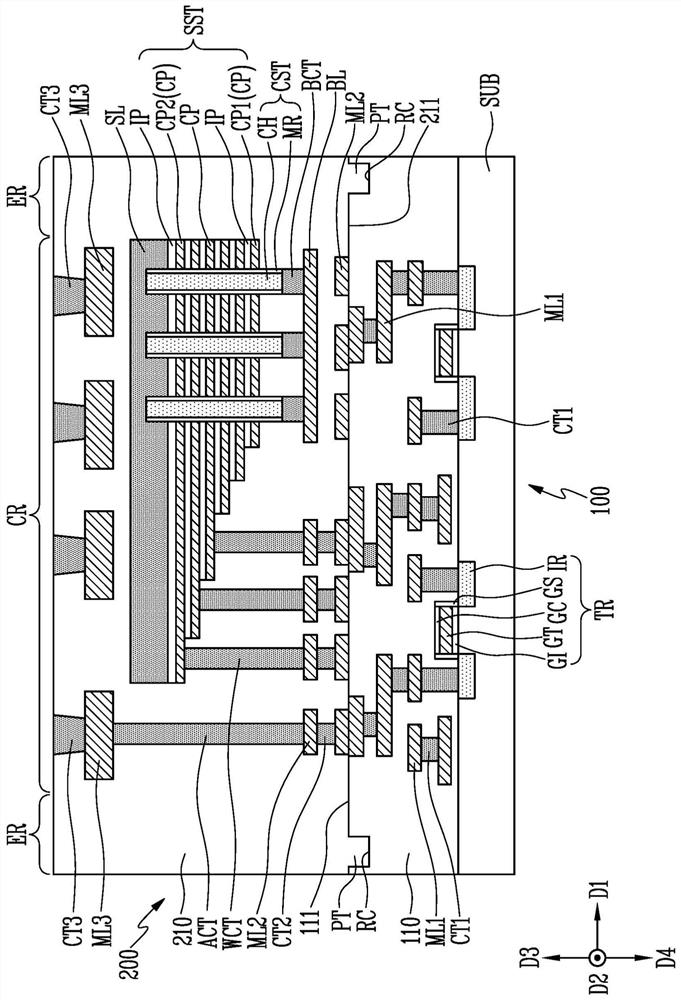
[0019] Figure 1A is a cross-sectional view of a semiconductor memory device according to an embodiment of the present disclosure. Figure 1B is instantiated Figure 1A A schematic plan view of the lower surface of the second chip. Figure 1C is instantiated Figure 1A A schematic plan view of the upper surface of the first chip.

[0020] refer to Figure 1A to Figure 1C , according to an embodiment of the p...


PUM


Abstract

A semiconductor memory device includes a first chip having a peripheral transistor and a first insulating layer, and includes a second chip having a stacked structure and a second insulating layer. The stacked structure includes conductive patterns and insulating patterns alternately stacked with each other, the first insulating layer includes a first bonding surface, the second insulating layer includes a second bonding surface contacting the first bonding surface, and the second chip further includes a protrusion protruding from the second bonding surface of the second insulating layer toward the first insulating layer.

Description

technical field [0001] Various embodiments relate generally to a semiconductor memory device, and more particularly to a three-dimensional semiconductor memory device. Background technique [0002] A semiconductor memory device may include memory cells capable of storing data. [0003] Depending on data storage and maintenance methods, semiconductor memory devices may be classified into volatile semiconductor memory devices and nonvolatile semiconductor memory devices. Volatile memory devices may lose data when power supply is interrupted, while non-volatile memory devices are capable of retaining stored data even without power supply. [0004] Recently, as the use of portable electronic devices has increased, the use of nonvolatile semiconductor memory devices has increased. Highly integrated semiconductor memory devices are being sought for portability and capacity. Three-dimensional semiconductor memory devices have been proposed to increase integration density. Cont...

Claims


Application Information

Patent Timeline
Patent Type & Authority Applications(China)
IPC IPC(8): H01L27/11521H01L27/11556H01L27/11568H01L27/11582
CPCH10B41/30H10B41/27H10B43/30H10B43/27H01L24/08H01L2224/05647H01L2224/05624H01L2224/05684H01L2224/80896H01L2224/80894H01L2224/80895H01L2224/80141H01L2224/0807H01L2224/0212H01L2224/80365H01L24/80H01L25/18H01L25/50H01L2225/06541H01L2225/06593H01L2224/08145H10B43/50H10B43/40H01L2924/00014H01L25/0657H01L23/31H01L23/485H01L23/525H01L24/16H01L2924/1434H01L2924/1431H01L2225/06524
Inventor 金镇河
Owner SK HYNIX INC
Features
  • R&D
  • Intellectual Property
  • Life Sciences
  • Materials
  • Tech Scout
  • Unparalleled Data Quality
  • Higher Quality Content
  • 60% Fewer Hallucinations
Learn More