A step-by-step printing device for photovoltaic crystalline silicon cells
What is AI technical title?
AI technical title is built by PatSnap AI team. It summarizes the technical point description of the patent document.
A printing device and crystalline silicon cell technology, which is applied in photovoltaic power generation, printing, printing presses, etc., can solve the problems of repeated busbar printing, reduce the electrical performance of photovoltaic crystalline silicon cells, etc., to avoid uneven printing and avoid replacement. Effect
Active Publication Date: 2022-03-25
徐州中辉光伏科技有限公司
View PDF7 Cites 1 Cited by
Summary
Abstract
Description
Claims
Application Information
AI Technical Summary
This helps you quickly interpret patents by identifying the three key elements:
Problems solved by technology
Method used
Benefits of technology
Problems solved by technology
[0003] The purpose of the present invention is to provide a step-by-step printing device for photovoltaic crystalline silicon cells to solve the problem of synchronizing the sub-grid and the main grid in the traditional printing process proposed in the background technology. Printing results in repeated printing of the busbar position, thereby reducing the electrical performance of photovoltaic crystalline silicon cells
Method used
Image
Click on the blue label to locate the original text in one second.
Reading with bidirectional positioning of images and text.
Examples
Embodiment Construction
[0031] The following will clearly and completely describe the technical solutions in the embodiments of the present invention with reference to the accompanying drawings in the embodiments of the present invention. Obviously, the described embodiments are only some, not all, embodiments of the present invention. Based on the embodiments of the present invention, all other embodiments obtained by persons of ordinary skill in the art without making creative efforts belong to the protection scope of the present invention.
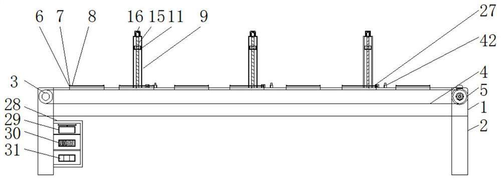
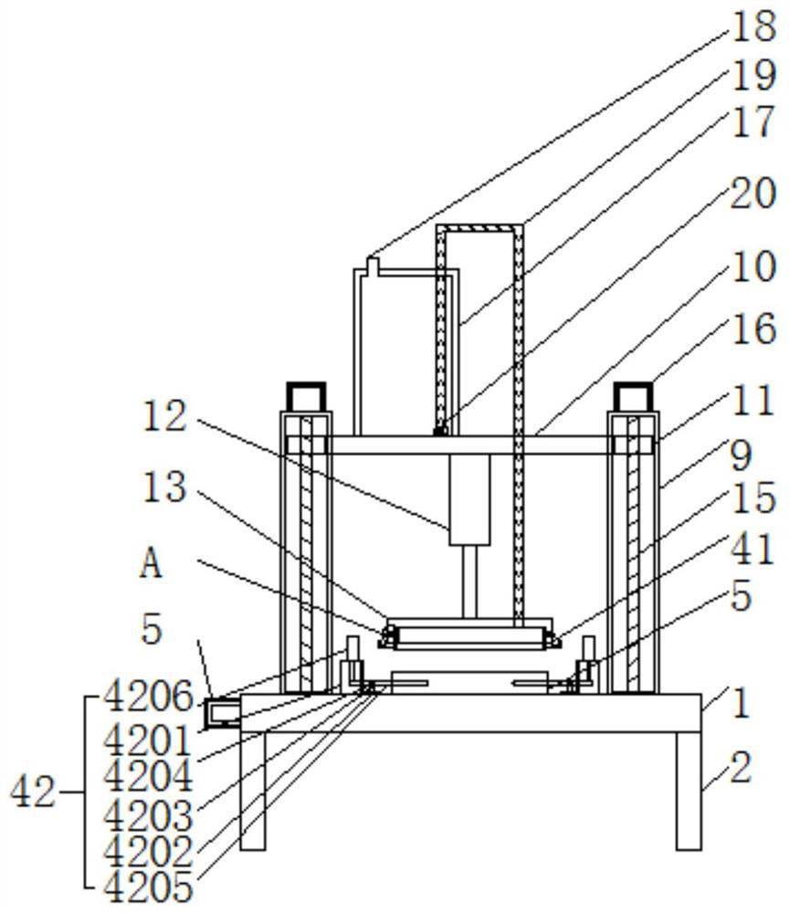
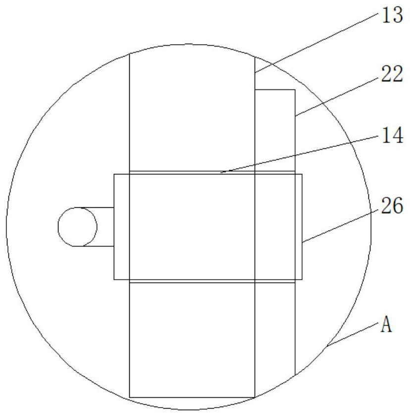
[0032] see Figure 1-10 , the present invention provides a technical solution: a step-by-step printing device for photovoltaic crystalline silicon cells, such as figure 1 , figure 2 , image 3 , Figure 4 , Figure 5 and Figure 10As shown, the bottom of the material ladder 1 is welded and fixed with the installation column 2, the inside of the material ladder 1 is installed with the roller shaft 3, the surface of the roller shaft 3 is rollingly connecte...
PUM
Abstract
The invention discloses a step-by-step printing device for photovoltaic crystalline silicon cells, which includes a material ladder, a placement plate, a first installation frame, a load-bearing plate, a clamping frame, a screw rod, a liquid barrel, an infusion tube, a clamping mold frame, and an infrared sensor , the first printing board, the second printing board, the third printing board, the card mold device and the limit printing device, the bottom of the material ladder is welded and fixed with the installation column, the top of the placement board is provided with a placement slot, and the first The installation frame is fixed on both sides of the top of the material ladder, wire blocks are fixed on both sides of the load-bearing plate, first clamping holes are opened on both sides of the clamping frame, and the step-by-step printing device of the photovoltaic crystal silicon cell is equipped with a first printing board, the second printing board, and the third printing board, it is convenient to print the main grid line, sub-grid line and auxiliary grid line through different printing boards, so as to avoid the duplication of position during the printing process of the main grid line due to the transformation of the overall crystalline silicon cell printing Printing, thereby reducing the electrical performance of the overall crystalline silicon cell.
Description
technical field [0001] The invention relates to the technical field of photovoltaic crystal silicon cells, in particular to a step-by-step printing device for photovoltaic crystal silicon cells. Background technique [0002] Photovoltaic crystalline silicon cells have always been developing toward improving conversion efficiency and reducing costs, but the optimization of the aspect ratio of the sub-grid lines in the existing photovoltaic crystalline silicon cell production process has received relatively great attention, but the traditional printing process will sub-grid The synchronous printing of the line and the main grid line will cause the printing of the main grid line position to be repeated, and at the same time reduce the electrical performance of the photovoltaic crystalline silicon cell. Contents of the invention [0003] The purpose of the present invention is to provide a step-by-step printing device for photovoltaic crystalline silicon cells to solve the pro...
Claims
Application Information
Patent Timeline
Application Date:The date an application was filed.
Publication Date:The date a patent or application was officially published.
First Publication Date:The earliest publication date of a patent with the same application number.
Issue Date:Publication date of the patent grant document.
PCT Entry Date:The Entry date of PCT National Phase.
Estimated Expiry Date:The statutory expiry date of a patent right according to the Patent Law, and it is the longest term of protection that the patent right can achieve without the termination of the patent right due to other reasons(Term extension factor has been taken into account ).
Invalid Date:Actual expiry date is based on effective date or publication date of legal transaction data of invalid patent.

