Wireless debugging system and method for embedded development board

A debugging system and development board technology, applied in control/regulation systems, general control systems, instruments, etc., can solve problems such as unfavorable batches, waste of USB interfaces, difficult log extraction, etc., to achieve low cost, increase convenience, and iteration efficiency Improved effect

Pending Publication Date: 2021-06-11
恒鸿达科技有限公司
View PDF7 Cites 0 Cited by
  • Summary
  • Abstract
  • Description
  • Claims
  • Application Information

AI Technical Summary

Problems solved by technology

However, in the case of high and low temperature experiments or outdoor tests, it is difficult to effectively extract logs in real time through wired connections
In addition, the wired connection method is inconvenient and wastes a USB interface or UART interface
Traditional general-purpose ARM chip debugging tools are expensive, which is not conducive to batch testing of copying machines

Method used


Image

  • Wireless debugging system and method for embedded development board
  • Wireless debugging system and method for embedded development board
  • Wireless debugging system and method for embedded development board

Examples


Embodiment Construction

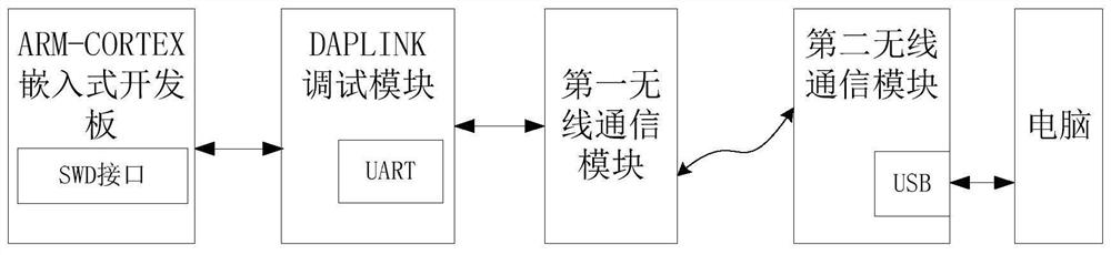
[0025] The embodiment of the present application provides a wireless debugging system and method for an embedded development board, and connects the wireless communication module through the DAPLINK debugging module, thereby increasing the convenience of debugging the embedded development board.

[0026] The general idea of ​​the technical solution in the embodiment of the application is as follows:

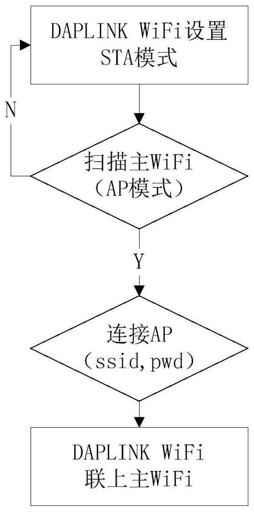
[0027] By transplanting the open source DAPLINK debugger + wireless WiFi module, the open source DAPLINK can be transplanted as long as it needs an ordinary ARM chip, which is lower than the price of purchasing Jlink. The SWD interface of the ARM-CORTEX series MCU is used to connect with the interface of the DAPLINK debugger. The first WiFi module (ie DAPLINKWiFi) is sent to the second WiFi module (ie the main WiFi module), and the second WiFi module is then transmitted to the computer through the USB interface, thereby realizing effective real-time debugging, updating system prog...


PUM


Abstract

The invention discloses a wireless debugging system for an embedded development board. The wireless debugging system comprises a DAPLINK debugging module, a first wireless communication module and a second wireless communication module; the DAPLINK debugging module is connected with an SWD interface of an embedded development board and is used for acquiring log data from the embedded development board or writing debugging data; the first wireless communication module is connected with the DAPLINK debugging module and is used for wirelessly transmitting and receiving data of the DAPLINK debugging module; the first wireless communication module is in wireless connection with the second wireless communication module; and the second wireless communication module is connected with a computer. According to the wireless debugging system and method for the embedded development board, the wireless communication module is connected through the DAPLINK debugging module, so that development debugging, log extraction and program updating of equipment are more convenient and simpler, and the development efficiency and the iteration efficiency are effectively improved.

Description

technical field [0001] The invention relates to the technical field of embedded devices, in particular to a wireless debugging system and method for an embedded development board. Background technique [0002] In the process of R&D, testing and production of embedded devices, in order to find and solve device problems, it is necessary to capture logs and debug the development board of embedded devices. [0003] The data transmission of the traditional embedded development board generally adopts a wired method, and the embedded development board and the computer are connected through the UART interface or the USB interface, so as to realize real-time capture of the logs of the embedded development board. However, in the case of high and low temperature experiments or outdoor tests, it is difficult to effectively extract logs in real time through wired connections. In addition, the wired connection method is extremely inconvenient and also wastes a USB interface or a UART int...

Claims


Application Information

Patent Timeline
IPC IPC(8): G05B19/042
CPCG05B19/0423G05B2219/25257
Inventor 林智铃
Owner 恒鸿达科技有限公司
Why Eureka
Try Eureka