A mass transfer method of micro LED chips and a display backplane

A transfer method and chip transfer technology, which is applied in semiconductor devices, electrical components, circuits, etc., can solve the problems of positional deviation and difficult effective electrical connection of MicroLED chips, and achieve effective electrical connection, high-precision mass transfer, and high efficiency. Effect

Active Publication Date: 2021-12-21
CHONGQING KONKA PHOTOELECTRIC TECH RES INST CO LTD
View PDF11 Cites 0 Cited by
  • Summary
  • Abstract
  • Description
  • Claims
  • Application Information

AI Technical Summary

Problems solved by technology

Mass transfer requires extremely high precision. If you are not careful, the position of the Micro LED chip will be shifted when it is bound to the light-emitting substrate, making it difficult to achieve an effective electrical connection between the Micro LED chip and the light-emitting substrate.

Method used


Image

  • A mass transfer method of micro LED chips and a display backplane
  • A mass transfer method of micro LED chips and a display backplane
  • A mass transfer method of micro LED chips and a display backplane

Examples


Embodiment Construction

[0066] In order to make the object, technical solution and advantages of the present invention more clear and definite, the present invention will be further described in detail below with reference to the accompanying drawings and examples. It should be understood that the specific embodiments described here are only used to explain the present invention, not to limit the present invention.

[0067] In the description of the present invention, it should be understood that the orientation or positional relationship indicated by the terms "center", "upper", "lower", "front", "rear", "left", "right" etc. are based on The orientations or positional relationships shown in the drawings are only for the convenience of describing the present invention and simplifying the description, and do not indicate or imply that the referred devices or components must have a specific orientation, be constructed and operated in a specific orientation, and therefore cannot be understood as Limitat...


PUM


Abstract

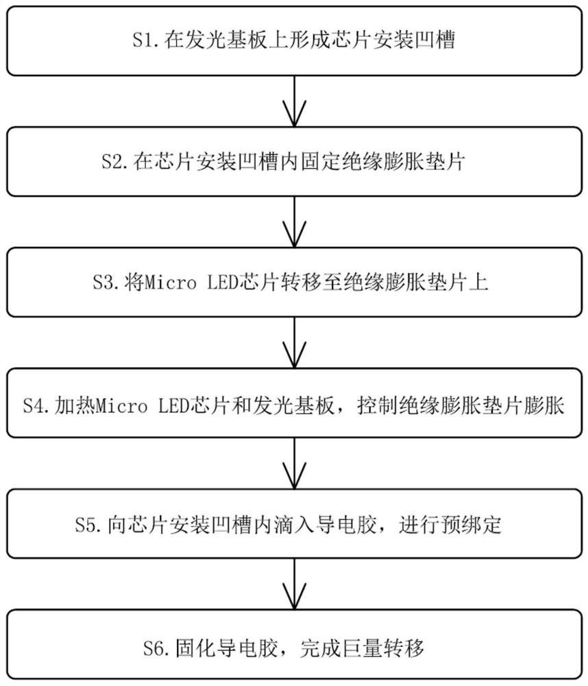
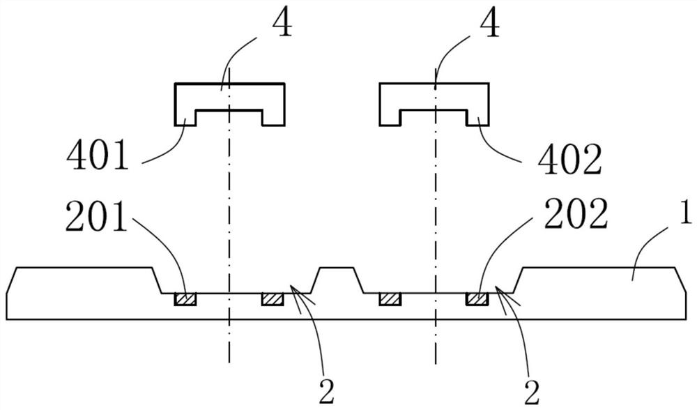
The present invention provides a method for transferring a large amount of Micro LED chips and a display backplane. First, an insulating expansion gasket is arranged in the chip mounting groove, and then the Micro LED chip is transferred to the insulating expansion gasket, and controlled by heating The regular expansion of the insulating expansion spacer realizes the alignment of the Micro LED chip, and can realize high-precision mass transfer with high efficiency, ensuring an effective electrical connection between the Micro LED chip and the light-emitting substrate. In the process of placing the Micro LED chip in the chip mounting groove, it is not necessary to strictly control the landing position of the Micro LED chip. It is only necessary to make the first chip electrode and the second chip electrode be located on both sides of the insulating expansion pad, and then By heating and controlling the regular expansion of the insulating expansion pad, the alignment of the Micro LED chip can be realized. At this time, further pre-binding and curing operations can ensure effective electrical connection between the Micro LED chip and the light-emitting substrate at low cost.

Description

technical field [0001] The present invention relates to the fields of semiconductor preparation equipment and light-emitting diode preparation equipment, relates to a method for mass transfer of Micro LED chips, and also relates to a display backplane produced by the above method. Background technique [0002] LED, that is, light-emitting diode, emits energy through the recombination of electrons and holes, and can efficiently convert electrical energy into light energy. It has many advantages and is considered to be the next generation of new solid-state light sources entering the field of general lighting. Micro LED is a new type of LED. Because of its many advantages such as fast response, high brightness, and low power consumption, it has high research and development value and use value. It has recently been welcomed by the market and favored by various manufacturers. [0003] In practical applications, a display backplane is composed of multiple Micro LED chips and a l...

Claims


Application Information

Patent Timeline
Patent Type & Authority Patents(China)
IPC IPC(8): H01L33/48H01L33/62H01L25/13
CPCH01L33/483H01L33/62H01L25/13H01L2933/0033H01L2933/0066
Inventor 李强许时渊
Owner CHONGQING KONKA PHOTOELECTRIC TECH RES INST CO LTD
Why Eureka
Try Eureka