
Method for improving ink precision through two times of printing

An ink and precision technology, applied in the field of improving ink precision by two printings, can solve the problems of ink overflow, existing ink, and low printing precision of ink, and achieve the effect of easy removal and improved precision.

Pending Publication Date: 2021-06-18
LEADER TECH ELECTRONICS SHENZHEN INC
View PDF9 Cites 1 Cited by
  • Summary
  • Abstract
  • Description
  • Claims
  • Application Information

AI Technical Summary

Problems solved by technology

However, due to the good fluidity of the ink in the existing method, the ink will overflow after printing and before it is baked and solidified, resulting in the phenomenon of ink in the non-ink printing area, and the printing accuracy of the ink is low.

Method used

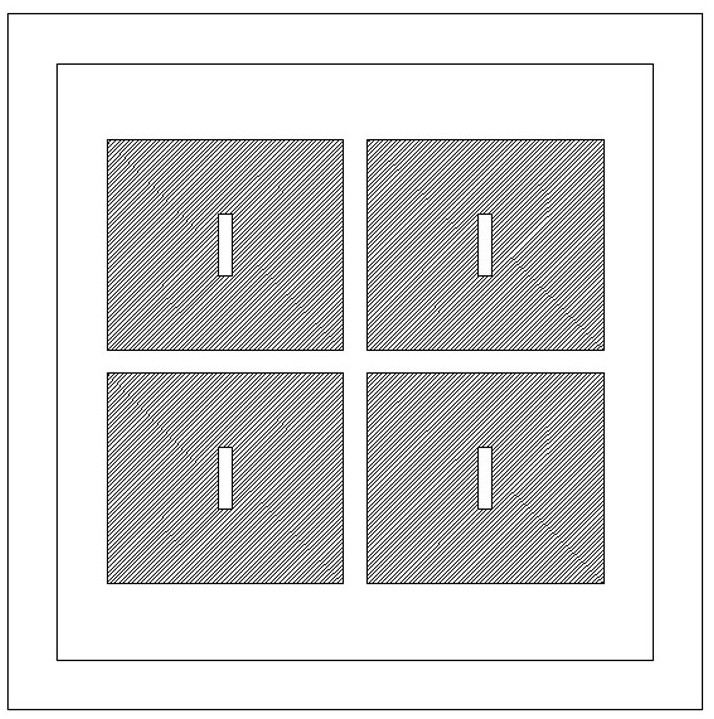
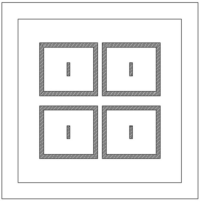
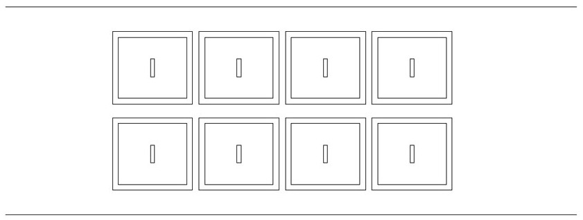

Image

  • Method for improving ink precision through two times of printing
  • Method for improving ink precision through two times of printing
  • Method for improving ink precision through two times of printing

Examples


Embodiment 1

[0034] Embodiment 1: two printings improve the method for printing ink precision, and this method comprises the following steps successively:

[0035] Step 1: According to the ink printing area and non-ink printing area of ​​the printed circuit board, respectively make ink printing screen and dam glue printing screen;

[0036] Step 2: Use dam glue and dam glue printing screen to print the product for the first time, so that the non-ink printing area is covered with dam glue;

[0037] Step 3: Use ink and ink printing screen to print the product for the second time, so that the ink printing area is covered with ink;

[0038] Step 4: Use pre-baking to preliminarily shape the ink;

[0039] Step 5: Remove the dam glue;

[0040] Step 6: Baking again to fully cure the ink.

Embodiment 2

[0041] Embodiment 2: two printings improve the method for printing ink precision, and this method comprises the following steps successively:

[0042] Step 1: According to the ink printing area and non-ink printing area of ​​the printed circuit board, respectively make ink printing screen and dam glue printing screen;

[0043] Step 2: Use dam glue and dam glue printing screen to print the product for the first time, so that the non-ink printing area is covered with dam glue;

[0044] Step 3: Use ink and ink printing screen to print the product for the second time, so that the ink printing area is covered with ink;

[0045] Step 4: Bake the ink to make the ink completely solidified;

[0046] Step 5: Remove the Dam Glue.


PUM


Abstract

The invention relates to a method for improving ink precision through two times of printing, and belongs to the technical field of printed circuit boards. The method comprises the following steps that an ink printing screen and a dam glue printing screen are manufactured according to an ink printing area and a non-ink printing area of a printed circuit board; the dam glue printing screen and the dam glue printing screen are adopted for conducting first-time printing on a product, and the non-ink printing area is fully coated with dam glue; the ink printing screen and the ink printing screen are adopted for conducting second-time printing on the product, and the ink printing area is fully coated with ink; and the ink is baked, and the ink is thoroughly cured; and the dam glue is removed. The method has the beneficial effects that two times of printing are adopted, after first-time printing, due to the poor fluidity of the dam glue, the specified non-ink area can be covered, after second-time ink printing is finished, due to the fact that the edge of the ink is blocked by the dam glue, the ink is covered in the specified ink printing area, and the ink overflow problem of a conventional ink printing technology cannot be caused; and the ink printing precision is improved.

Description

technical field [0001] The invention relates to a method for improving ink precision by double printing, and belongs to the technical field of printed circuit boards. Background technique [0002] In today's society, science and technology are changing with each passing day, and people's thinking is also changing rapidly. From the existence of no electronic products in life to the ubiquitous electronic products in life, as people's use of electronic products increases, the electronics industry has also gained With the rapid development, the printed circuit board industry has also developed rapidly. High-efficiency, high-quality, and low-cost production has always been the goal of the printed circuit board industry. [0003] Aiming at this goal, this patent provides a method for improving ink precision by printing twice, by printing dam glue on the non-ink printing area and printing ink on the printing area twice to prevent ink overflow and improve ink printing accuracy. [...

Claims


Application Information

Patent Timeline
Patent Type & Authority Applications(China)
IPC IPC(8): B41M3/00B41M1/12
CPCB41M3/00B41M1/12
Inventor 韩少华王健孙彬沈洪李晓华
Owner LEADER TECH ELECTRONICS SHENZHEN INC
Learn More