
Patsnap Eureka
For R&D, Patsnap Eureka makes reading and utilizing patents & technical documents easy.
Patsnap Eureka AIR
Designed for self-driven R&D workflows. Generate viable solutions, solve complex R&D challenges, empower your innovation with AI.

Patsnap Eureka Materials
Designed for material experts only. Revolutionize your material R&D, from search, analyze, to developing new materials.

TechResearch
Generate reliable direction feasibility study reports for your R&D in just a few steps.

TechSeek
Discover and master advanced knowledge NOW. Basics, ideas, possibilities, all at once.

TechMind
As an expert in R&D Theories, TechMind can generates customized viable solutions instantly.

TechRisk
Analyze your overall solution with one click, know your potential R&D risks in advance.

TechMonitor
Get weekly tech updates, stay abreast of the latest tech innovations and key insights.
Image sensor device and manufacturing method thereof
An image sensor and device technology, applied in the direction of electric solid devices, semiconductor devices, electrical components, etc., can solve the problems of capillary force influence and aggravation
- Summary
- Abstract
- Description
- Claims
- Application Information
AI Technical Summary
Problems solved by technology
Method used
Image

Examples
example 1
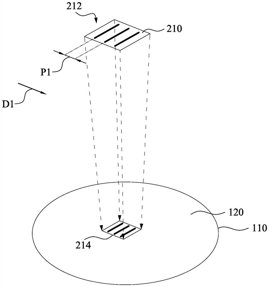
[0097] Example 1. A method for fabricating an image sensor device comprising: forming a first photoresist layer on a front side of a device substrate, wherein the first photoresist layer has spaced apart a first trench; performing a first implantation process using the first photoresist layer as a mask to form a first isolation region in the device substrate; forming on the front side of the device substrate a second photoresist layer, wherein the second photoresist layer has second grooves spaced apart from each other; performing a second implant using the second photoresist layer as a mask process to form a second isolation region in the device substrate and intersecting the first isolation region; and form a third photoresist layer on the front side of the device substrate, wherein the The third photoresist layer has third grooves spaced apart from each other; using the third photoresist layer as a mask to perform a third implantation process in the device substrate and wit...
example 2
[0098] Example 2. The method of example 1, wherein the second grooves of the second photoresist layer have a first pitch and the third grooves of the third photoresist layer have a a second pitch that is the same as the first pitch.
example 3
[0099] Example 3. The method of example 2, wherein the first pitch is greater than 1 micron.
PUM
| Property | Measurement | Unit |
|---|---|---|
| width | aaaaa | aaaaa |
| length | aaaaa | aaaaa |
Abstract
Description
Claims
Application Information
 - R&D Engineer
- R&D Manager
- IP Professional
- Industry Leading Data Capabilities
- Powerful AI technology
- Patent DNA Extraction
Browse by: Latest US Patents, China's latest patents, Technical Efficacy Thesaurus, Application Domain, Technology Topic, Popular Technical Reports.
© 2024 PatSnap. All rights reserved.Legal|Privacy policy|Modern Slavery Act Transparency Statement|Sitemap|About US| Contact US: help@patsnap.com