Component carrier manufacturing method, processing system, computer program and system architecture

A technology of component loading and semi-finished products, applied in the field of system architecture, can solve problems such as system false detection

Active Publication Date: 2021-06-25
AT&S (CHONGQING) CO LTD
View PDF14 Cites 1 Cited by
  • Summary
  • Abstract
  • Description
  • Claims
  • Application Information

AI Technical Summary

Problems solved by technology

However, known systems still generate a large number of false detection defects

Method used


Image

  • Component carrier manufacturing method, processing system, computer program and system architecture
  • Component carrier manufacturing method, processing system, computer program and system architecture
  • Component carrier manufacturing method, processing system, computer program and system architecture

Examples


Embodiment Construction

[0093] The illustrations in the figures are schematic. It should be noted that in different figures, similar or identical elements or features are provided with the same reference signs or with reference signs that differ from the corresponding reference signs only within the first digit . In order to avoid unnecessary repetition, elements or features that have already been explained with respect to the previously described embodiments will not be described in detail later in this specification.

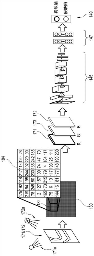
[0094] figure 1 Algorithms are shown for AI processing of AOI captured images to identify false defects that have been detected by undelineated AOI devices on the surface of a semi-finished part carrier. The described algorithm relying on AOI defect detection can be executed for each layer of the multi-layer component carrier. Such a multilayer component carrier can be formed by sequentially laminating an electrically conductive layer structure and an electrically insulating layer...


PUM


Abstract

A component carrier manufacturing method and a system for processing a component carrier are described. The method includes: (a) supplying the semi-finished part carrier to an automated optical inspection device; (b) performing an automated optical inspection of the semi-finished part carrier, comprising the steps of: capturing a first image by a first illumination; capturing a second image by the second illumination; comparing an actual data set indicative of the first image and / or the second image with a reference data set; identifying potential defects; (c) performing a quality classification of the semi-finished part carrier, comprising the steps of: generating a virtual third image indicative of the semi-finished part carrier in the case of a virtual third illumination, the third spectral component being different from both the first spectral component and the second spectral component; processing the three images, and classifying the identified potential defects; (d) taking an action based on the quality classification performed. A system architecture is also described.

Description

technical field [0001] The invention relates generally to the technical field of manufacturing component carriers. In particular, the invention relates to a method for manufacturing a component carrier, in which method a quality classification of semi-finished products of the component carrier is carried out by means of artificial intelligence processing. Furthermore, the invention relates to a system architecture for classifying defects of semi-finished component carriers during the manufacture of the component carrier. Background technique [0002] The electronic function of a component carrier equipped with one or more electronic components continues to increase, and the miniaturization of such electronic components continues to increase, and the electronics to be mounted on a component carrier such as a printed circuit board (PCB) Against the backdrop of an ever-increasing number of components, increasingly powerful array-like components or packages are being used with ...

Claims


Application Information

Patent Timeline
IPC IPC(8): G06F30/17G06F30/27G06F119/02
CPCG06F30/17G06F30/27G06F2119/02G06T2207/30141G06T7/001G06T7/0004G06T2207/20084G06T11/001G01N21/95607G01N21/95684G01N2021/8883G01N2021/8887G06N20/00G06V2201/06G06V10/764G01N21/95G01N35/00584G06T11/00G06T2207/10152G06T2207/20081
Inventor 王勇万学兵陈彦旭陈洋林涛
Owner AT&S (CHONGQING) CO LTD
Why Eureka
Try Eureka