Semiconductor package
A technology for semiconductors and packages, which is applied in the field of semiconductor packages with heat dissipation characteristics, and can solve problems such as performance degradation of semiconductor packages
- Summary
- Abstract
- Description
- Claims
- Application Information
AI Technical Summary
Problems solved by technology
Method used
Image

Examples
Embodiment Construction
[0025] Hereinafter, various exemplary embodiments will be described in detail with reference to the accompanying drawings. Like reference numerals refer to like elements throughout, and a previously given description will be omitted for the sake of brevity.
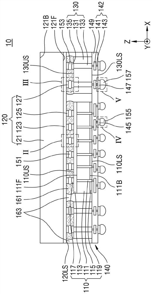
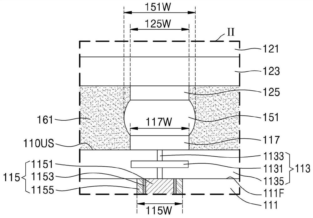
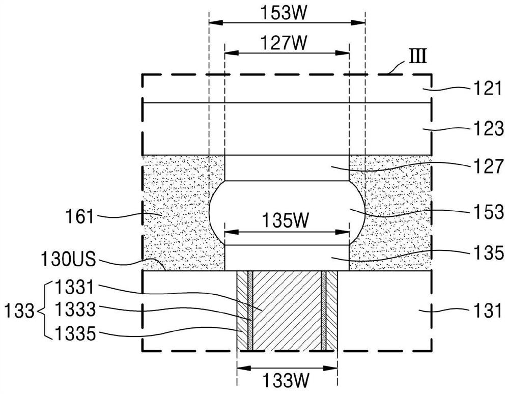
[0026] figure 1 is a cross-sectional view illustrating a semiconductor package 10 according to various exemplary embodiments. figure 2 is shown figure 1 The enlarged cross-sectional view of region II in . image 3 is shown figure 1 An enlarged cross-sectional view of region III in . Figure 4 is shown figure 1 An enlarged cross-sectional view of region IV in . Figure 5 is shown figure 1 An enlarged cross-sectional view of region V in .
[0027] refer to Figure 1 to Figure 5 , the semiconductor package 10 may include a lower semiconductor device 110 , an upper semiconductor device 120 , a connection substrate 130 , a first molding layer 163 and a first redistribution structure 140 .
[0028] The upper semicond...
PUM
 Abstract
Description
Claims
Application Information
 - R&D
- Intellectual Property
- Life Sciences
- Materials
- Tech Scout
- Unparalleled Data Quality
- Higher Quality Content
- 60% Fewer Hallucinations
Browse by: Latest US Patents, China's latest patents, Technical Efficacy Thesaurus, Application Domain, Technology Topic, Popular Technical Reports.
© 2025 PatSnap. All rights reserved.Legal|Privacy policy|Modern Slavery Act Transparency Statement|Sitemap|About US| Contact US: help@patsnap.com