Semiconductor device and preparation method thereof

A semiconductor and device technology, applied in the field of semiconductor devices and their preparation, can solve problems such as time-consuming, photoresist stripping, and cost increase, and achieve the effects of improving product performance, low cost, and ensuring uniformity

Inactive Publication Date: 2021-07-09
晶芯成(北京)科技有限公司
View PDF6 Cites 0 Cited by
  • Summary
  • Abstract
  • Description
  • Claims
  • Application Information

AI Technical Summary

Problems solved by technology

In addition, it is also prone to problems such as photoresist stripping
In order to solve these side effects, only by upgrading the equipment or replacing the photoresist, it will not only increase the cost, but also take a lot of time

Method used


Image

  • Semiconductor device and preparation method thereof
  • Semiconductor device and preparation method thereof
  • Semiconductor device and preparation method thereof

Examples


preparation example Construction

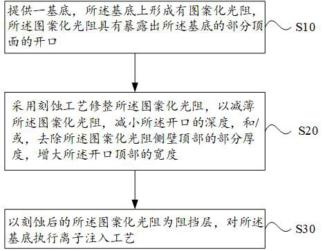
[0039] In order to solve the above technical problems, this embodiment provides a method for manufacturing a semiconductor device, please refer to image 3 ,include:

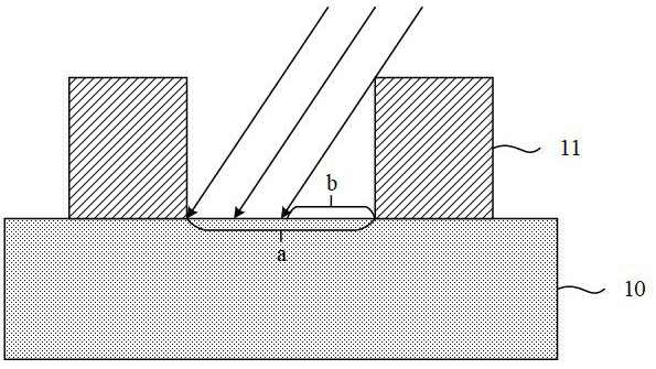
[0040] Step 1 S10: providing a substrate, on which a patterned photoresist is formed, and the patterned photoresist has an opening exposing part of the top surface of the substrate;

[0041] Step 2 S20: trimming the patterned photoresist by using an etching process to thin the patterned photoresist, reduce the depth of the opening, and / or remove the top part of the patterned photoresist sidewall thickness, increasing the width of the top of the opening;

[0042] Step 3 S30: Using the etched patterned photoresist as a barrier layer, perform an ion implantation process on the substrate.

[0043] In this embodiment, the size of the patterned photoresist is adjusted by etching and trimming, so as to at least reduce the thickness of the patterned photoresist, and / or increase the width of the top of the opening, so ...


PUM

PropertyMeasurementUnit
Thicknessaaaaaaaaaa

Abstract

The invention provides a semiconductor device and a preparation method thereof. The size of the patterned photoresist is adjusted by adopting an etching trimming mode so as to realize thinning of the patterned photoresist and / or increase of the width of the top of the opening, so that the shadow effect occurring in the subsequent ion implantation process can be relieved, namely, the shielding area is reduced, the ion implantation range is expanded, the uniformity of ion implantation is ensured, and the product performance is improved. Moreover, compared with a thinning mode of yellow light irradiation, side effects such as substrate defects or photoresist stripping can be avoided, the method is not limited by photoresist or machine characteristics, and the thickness of the patterned photoresist thinned in an etching finishing mode can be smaller than a limit value of yellow light thinning, so that a better process effect is achieved. In addition, compared with replacement of a light resistor or upgrading of a machine, the method is low in cost, easy to operate and high in feasibility.

Description

technical field [0001] The invention relates to the technical field of semiconductor device manufacturing, in particular to a semiconductor device and a preparation method thereof. Background technique [0002] At present, in the field of semiconductor technology, the ion implantation process is an essential material surface modification technology. The basic principle is: use an ion beam with an energy of 100keV to enter the material, a series of physical and chemical interactions will occur between the ion beam and the atoms or molecules in the material, the incident ions will gradually lose energy, and finally stay in the In the material, and cause changes in the surface composition, structure and properties of the material, thereby optimizing the surface properties of the material, or obtaining some new excellent properties. Due to its unique and prominent advantages, this technology has been widely used in the doping of semiconductor materials and the surface modificat...

Claims


Application Information

Patent Timeline
IPC IPC(8): H01L21/266
CPCH01L21/266
Inventor 张静许宗能
Owner 晶芯成(北京)科技有限公司
Why Eureka
Try Eureka