
TP chip scanning method for improving point reporting accuracy

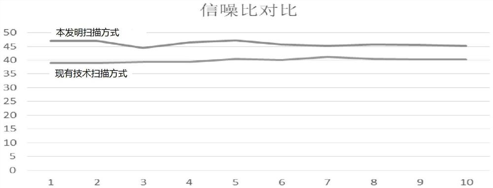
A scanning method and accuracy technology, which is applied in the field of TP chips, can solve the problems of uneven data collection and low accuracy of TP chip report points, and achieve increased report point accuracy, increased signal-to-noise ratio, and obvious signal-to-noise ratio Effect

Inactive Publication Date: 2021-07-23
合肥松豪电子科技有限公司
View PDF5 Cites 0 Cited by
  • Summary
  • Abstract
  • Description
  • Claims
  • Application Information

AI Technical Summary

Problems solved by technology

[0004] In order to solve the problem of low accuracy of TP chip report points caused by the uneven data collection of the two channels adjacent to the triangular screen body, the present invention provides a TP chip scanning method that increases the accuracy of report points. The specific scheme is as follows:

Method used


Image

  • TP chip scanning method for improving point reporting accuracy
  • TP chip scanning method for improving point reporting accuracy
  • TP chip scanning method for improving point reporting accuracy

Examples


Embodiment Construction

[0019] In order to make the purpose, technical solutions and advantages of the embodiments of the present invention more clear, the technical solutions in the embodiments of the present invention will be clearly and completely described below in conjunction with the accompanying drawings in the embodiments of the present invention. Obviously, the described embodiments It is a part of embodiments of the present invention, but not all embodiments. Based on the embodiments of the present invention, all other embodiments obtained by persons of ordinary skill in the art without making creative efforts belong to the protection scope of the present invention.

[0020] The invention discloses a TP chip scanning method for increasing the reporting accuracy, comprising the following steps:

[0021] The working method of the present invention is described in conjunction with accompanying drawings.

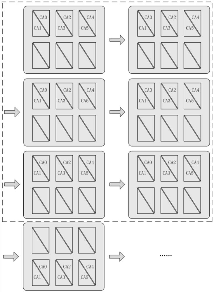
[0022] Such as Figure 4 As shown, 6 charge amplifiers are used, respectively labeled a...


PUM


Abstract

The invention relates to the technical field of TP chips, in particular to a TP chip scanning method for improving point reporting accuracy. Each charge amplifier carries out data acquisition on each channel needing acquisition. The TP chip has the advantages that the technical process offset of the charge amplifier and the capacitance mismatch of the channel capacitor are counteracted, and the point reporting accuracy of the TP chip is improved.

Description

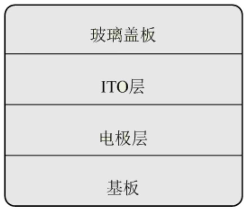
technical field [0001] The invention relates to the technical field of TP chips, in particular to a TP chip scanning method for increasing reporting accuracy. Background technique [0002] Capacitive touch screens, such as figure 1 Shown mainly consists of 4 parts. The uppermost layer is a glass cover, and channels on the cover are generally cut out according to the rules, and users can realize human-computer interaction by touching the channels. The second layer is the ITO layer, and the ITO wiring matches the channel pattern and position cut by the glass cover. According to the ITO wiring, the electrodes of each channel are built to form the electrode layer. In the electrode layer, the electrode and the ground form a self-capacitance. When a finger is touched, the capacitance of the human finger will be coupled to the self-capacitance. TPIC determines whether there is a finger touch by continuously detecting the capacitance data of each channel. And determine where the...

Claims


Application Information

Patent Timeline
Patent Type & Authority Applications(China)
IPC IPC(8): G06F3/041G06F3/044
CPCG06F3/04186G06F3/04166G06F3/044
Inventor 杜洪洋张金磊黄俊钦
Owner 合肥松豪电子科技有限公司
Learn More