Transfer head, transfer device and transfer method

A transfer device and transfer head technology, which is applied in the manufacturing of electrical components, circuits, semiconductor/solid-state devices, etc., can solve the problems of low yield of mass transfer, inability to meet chip pickup and release at the same time, and poor transfer ability of transfer heads, etc. Achieve the effect of preventing chips from falling off, strong transfer ability, and improving yield

Pending Publication Date: 2021-08-03
CHENGDU VISTAR OPTEOLECTRONICS CO LTD
View PDF5 Cites 0 Cited by
  • Summary
  • Abstract
  • Description
  • Claims
  • Application Information

AI Technical Summary

Problems solved by technology

However, the transfer capability of the existing transfer heads is poor, and cannot meet the needs of chip pick-up and release at the same time, resulting in a low yield of mass transfer

Method used


Image

  • Transfer head, transfer device and transfer method
  • Transfer head, transfer device and transfer method
  • Transfer head, transfer device and transfer method

Examples


Embodiment Construction

[0050] The present invention will be further described in detail below in conjunction with the accompanying drawings and embodiments. It should be understood that the specific embodiments described here are only used to explain the present invention, but not to limit the present invention. In addition, it should be noted that, for the convenience of description, only some structures related to the present invention are shown in the drawings but not all structures.

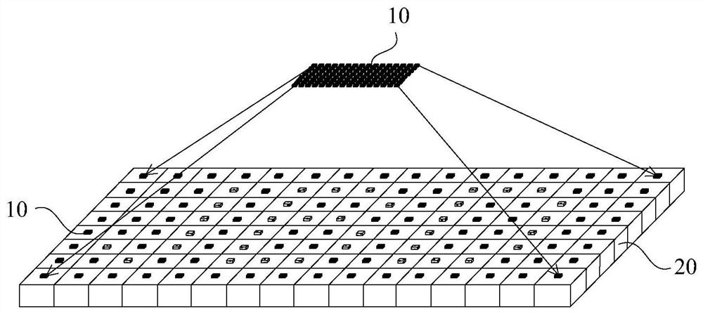
[0051] As mentioned in the background technology, the transfer ability of the existing transfer head is poor and cannot meet the requirements of pick-up and release at the same time. The reason for this problem will be analyzed below by taking the transfer of micro-LED chips to the backplane as an example. figure 1 It is a schematic diagram of transferring micro-LED chips to the backplane. see figure 1 , reference numeral 10 represents a chip, such as a micro-LED chip; reference numeral 20 represents a backplane,...


PUM


Abstract

The embodiment of the invention discloses a transfer head, a transfer device and a transfer method. The transfer head includes: a substrate; and a plurality of transfer parts, wherein the transfer parts are located on the substrate, each transfer part comprises a transfer bonding surface far away from one side of the substrate, the transfer bonding surfaces are used for being bonded with the chip, and the bonding force between the transfer bonding surface and the chip is adjustable. Compared with the prior art, different requirements of chip picking and releasing on the transfer head can be met at the same time, and the transfer capacity of the transfer head is improved.

Description

technical field [0001] The embodiments of the present invention relate to the field of display technology, and in particular to a transfer head, a transfer device and a transfer method. Background technique [0002] With the development of display technology, the display mode has gradually developed from cathode ray tube (Cathode Ray Tube, CRT), liquid crystal display (Liquid Crystal Display), organic light-emitting diode display (Organic Light-Emitting Diode, OLED) to micro-light-emitting diode display (Micro light-emitting diode display). Light Emitting Diode, Micro LED). [0003] Among them, Micro-LED display technology has the advantages of high brightness, high response speed, low power consumption and long life, and has become a research hotspot in the new generation of display technology. In the process of preparing Micro-LED display panels, the commonly used technology is mass transfer technology, which specifically uses a transfer head to pick up and release Micro-...

Claims


Application Information

Patent Timeline
Patent Type & Authority Applications(China)
IPC IPC(8): H01L21/683H01L21/67
CPCH01L21/683H01L21/67144
Inventor 宋玉华董小彪韩赛赛王岩姚志博
Owner CHENGDU VISTAR OPTEOLECTRONICS CO LTD
Why Eureka
Try Eureka