High-barrier spunbonded new semiconductor material preparation equipment
A technology for semiconductors and new materials, applied in the field of high-barrier spunbond semiconductor new material preparation equipment, can solve problems such as increasing the workload of personnel
- Summary
- Abstract
- Description
- Claims
- Application Information
AI Technical Summary
Problems solved by technology
Method used
Image
Examples
Embodiment 1
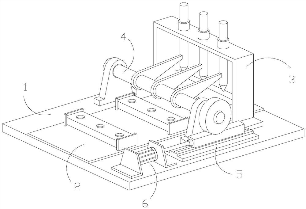
[0031] as attached figure 1 to attach Figure 6 Shown:
[0032] The invention provides a high-barrier spun-bonded semiconductor new material preparation equipment, the structure of which is provided with a bottom plate 1, a material setting plate 2, an operation frame 3, a control frame 4, a guide rail 5, and a motor 6, and the material setting plate 2 is fixedly installed On the top of the base plate 1, the operating frame 3 is slidably connected to the base plate 1, the control frame 4 is connected to the side of the operating frame 3 and movably matched, the control frame 4 is slidably connected to the guide rail 5, and the motor 6 is installed at one side above the bottom plate 1.
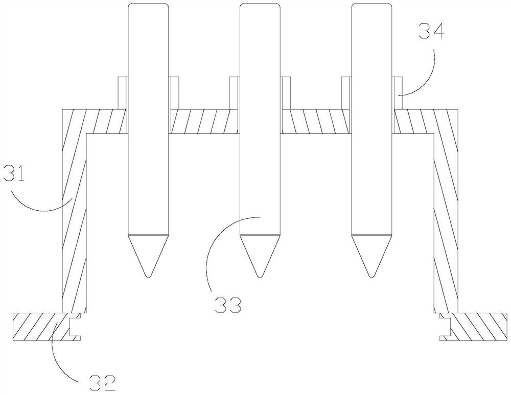
[0033] The operating frame 3 is provided with a support frame 31, a clamping plate 32, a punching device 33, and a guide post 34. The clamping plate 32 is embedded and connected to both sides of the lower end of the support frame 31, and the guide post 34 is installed on the support frame. A...
Embodiment 2
[0040] as attached Figure 7 to attach Figure 9 Shown:
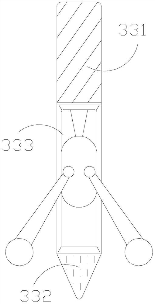
[0041] Wherein, the abutting frame a2 is provided with an connecting rod a21 and a pressing ball a22, the abutting ball a22 is embedded and connected to the lower end of the connecting rod a21 and is movably matched, and the connecting rod a21 can perform hinged swinging movement, so The pressing ball a22 has a spherical structure, and the pressing ball a22 moves under the drive of the connecting rod a21 to generate a pressing force on the material below.
[0042] Wherein, the pressing ball a22 is provided with an upper end block w1, a cavity w2, a lower frame w3, and a port w4, the cavity w2 is located below the upper end block w1, and the lower frame w3 is integrated with the upper end block w1 structure and located below it, the opening w4 is set through the lower frame w3, the inside of the cavity w2 is in the state of a certain space, the opening w4 is in a transparent state, and the diameter width is from the in...
PUM
 Abstract
Description
Claims
Application Information
 - R&D
- Intellectual Property
- Life Sciences
- Materials
- Tech Scout
- Unparalleled Data Quality
- Higher Quality Content
- 60% Fewer Hallucinations
Browse by: Latest US Patents, China's latest patents, Technical Efficacy Thesaurus, Application Domain, Technology Topic, Popular Technical Reports.
© 2025 PatSnap. All rights reserved.Legal|Privacy policy|Modern Slavery Act Transparency Statement|Sitemap|About US| Contact US: help@patsnap.com


