Mold forming device for High-power semiconductor device package

A device packaging and mold forming technology, which is applied in semiconductor/solid-state device manufacturing, electrical components, household components, etc., can solve problems such as product damage, difficulty in demoulding molded products, affecting product molding effect and molding quality, etc.

Pending Publication Date: 2021-08-13
龚小华
View PDF0 Cites 0 Cited by
  • Summary
  • Abstract
  • Description
  • Claims
  • Application Information

AI Technical Summary

Problems solved by technology

[0003] When molding a high-power semiconductor device package, the material is injected into the mold for molding. During the molding process, the injection material will stick to the mold, and it is necessary to rely on the staff to manually pull out the molded product from the mold core. The demoulding makes it very difficult to demould the molded product, and the product will be pulled during manual demoulding, causing the molded product to be damaged and scrapped, affecting the molding effect and molding quality of the product

Method used


Image

  • Mold forming device for High-power semiconductor device package
  • Mold forming device for High-power semiconductor device package
  • Mold forming device for High-power semiconductor device package

Examples


Embodiment 1

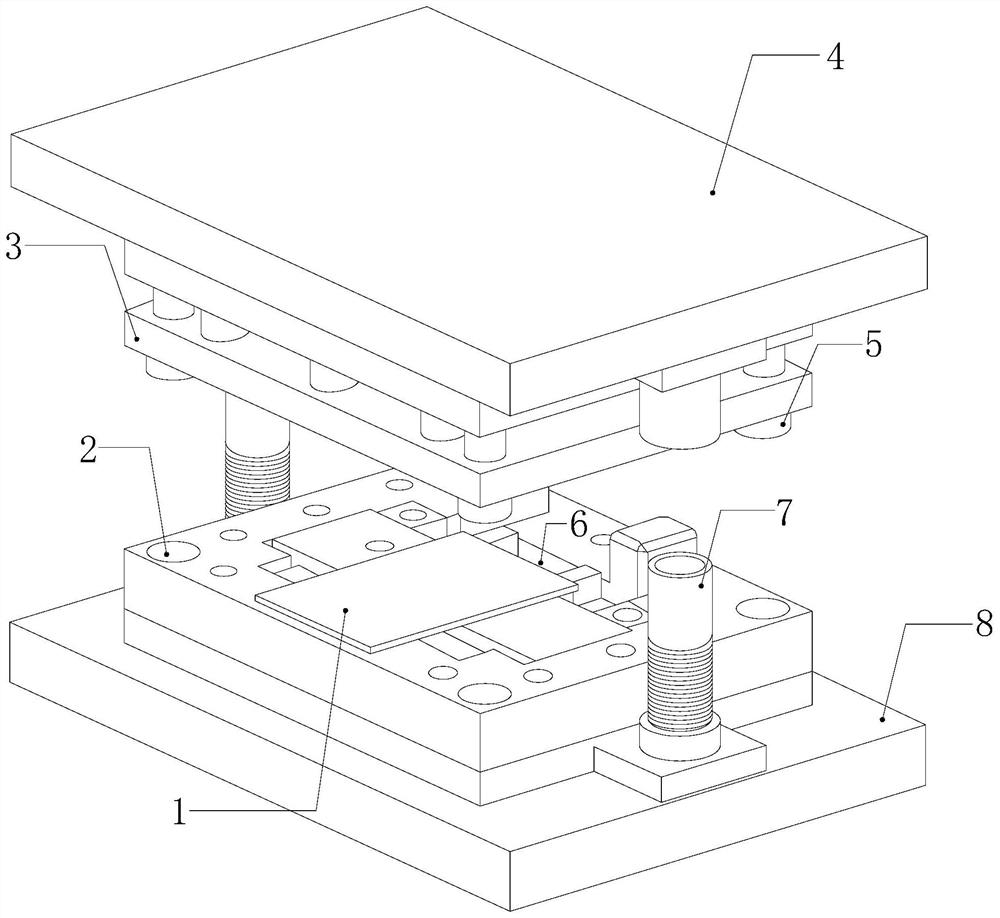
[0029] see figure 1 , the present invention provides a technical solution: a high-power semiconductor device packaging mold molding device, the structure of which includes a lower mold core 1, a docking hole 2, an upper mold core 3, an upper mold 4, a docking rod 5, an ejector device 6, Position bar 7, lower mold 8, described lower mold core 1 is installed on the lower mold 8, is provided with ejection device 6 between described lower mold 8 and lower mold core 1, and described lower mold 8 both sides are all provided with The connecting positioning rod 7, the lower die 8 is connected with the upper die 4 through the positioning rod 7, the upper die 4 is integrated with the upper die core 3, and the upper die 4 is provided with a butt joint rod 5, The docking rod 5 is socketed with the docking hole 2 through the upper mold 4 , and the lower mold core 1 and the upper mold core 3 are closely attached.

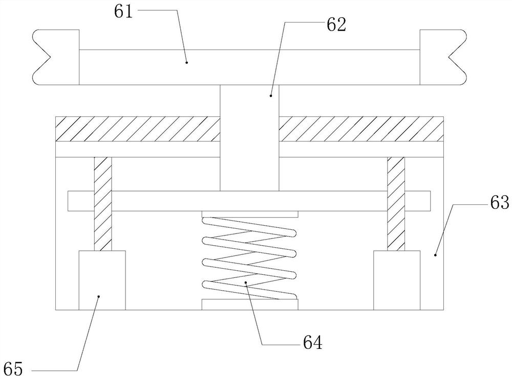
[0030] see figure 2 , the ejector device 6 includes a clamping member 61...

Embodiment 2

[0040] see figure 1 , the present invention provides a technical solution: a high-power semiconductor device packaging mold molding device, the structure of which includes a lower mold core 1, a docking hole 2, an upper mold core 3, an upper mold 4, a docking rod 5, an ejector device 6, Position bar 7, lower mold 8, described lower mold core 1 is installed on the lower mold 8, is provided with ejection device 6 between described lower mold 8 and lower mold core 1, and described lower mold 8 both sides are all provided with The connecting positioning rod 7, the lower die 8 is connected with the upper die 4 through the positioning rod 7, the upper die 4 is integrated with the upper die core 3, and the upper die 4 is provided with a butt joint rod 5, The docking rod 5 is socketed with the docking hole 2 through the upper mold 4 , and the lower mold core 1 and the upper mold core 3 are closely attached.

[0041] see figure 2 , the ejector device 6 includes a clamping member 61...


PUM


Abstract

The invention discloses a mold forming device for high-power semiconductor device package. The device structurally comprises a lower mold core, a butt joint hole, an upper mold core, an upper mold, a butt joint rod, an ejection device, a positioning rod and a lower mold. When the device is used, a clamping piece is fixedly connected with the lower mold core, a material is injected onto the lower mold core, the upper mold core on the upper mold and the lower mold core on the lower mold can be accurately butted together to perform extrusion forming on the material, after a product is formed, the upper mold is opened, a movable rod is ejected upwards under the cooperation of a spring and a sliding fixed piece, the clamping piece can drive the lower mold core to move upwards under the action of the movable rod, the formed product on the lower mold core is ejected upwards, therefore, a worker can quickly demould the formed product on the lower mold core, and the forming effect and the forming quality of the formed product are improved.

Description

technical field [0001] The invention relates to the field of high-power semiconductor devices, in particular to a packaging mold molding device for high-power semiconductor devices. Background technique [0002] With the rapid development of science and technology, power semiconductor devices are developing in the direction of high power, high frequency, and integration. Power semiconductor devices have various structures, so they are widely used. High-power semiconductor devices are used in almost all electronic manufacturing industries. , including notebooks, PCs, servers, monitors and various peripherals in the computer field, the formed mold is ejected upward through the ejector element. When performing mold molding, the areas that need to be improved: [0003] When molding a high-power semiconductor device package, the material is injected into the mold for molding. During the molding process, the injection material will stick to the mold, and it is necessary to rely on...

Claims


Application Information

Patent Timeline
Patent Type & Authority Applications(China)
IPC IPC(8): B29C45/26B29C45/40B29C45/14H01L21/56B29L31/34
CPCB29C45/14B29C45/2602B29C45/4005B29L2031/34H01L21/565
Inventor 龚小华
Owner 龚小华
Why Eureka
Try Eureka