
Eureka
For R&D, Eureka makes reading and utilizing patents & technical documents easy.
Eureka AIR
Designed for self-driven R&D workflows. Generate viable solutions, solve complex R&D challenges, empower your innovation with AI.

Eureka Materials
Designed for material experts only. Revolutionize your material R&D, from search, analyze, to developing new materials.

TechResearch
Generate reliable direction feasibility study reports for your R&D in just a few steps.

TechSeek
Discover and master advanced knowledge NOW. Basics, ideas, possibilities, all at once.

TechMind
As an expert in R&D Theories, TechMind can generates customized viable solutions instantly.

TechRisk
Analyze your overall solution with one click, know your potential R&D risks in advance.

TechMonitor
Get weekly tech updates, stay abreast of the latest tech innovations and key insights.
Semiconductor storage device and manufacturing method thereof
A storage device and semiconductor technology, applied in semiconductor/solid-state device manufacturing, semiconductor devices, semiconductor/solid-state device components, etc., can solve problems that are contrary to the miniaturization of memory cell arrays
- Summary
- Abstract
- Description
- Claims
- Application Information
AI Technical Summary
Problems solved by technology
Method used
Image

Examples
no. 1 Embodiment approach
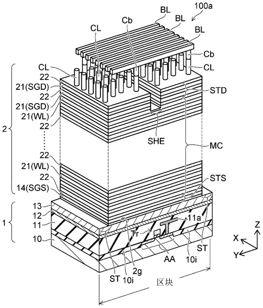
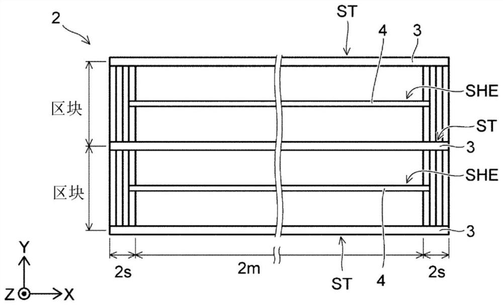
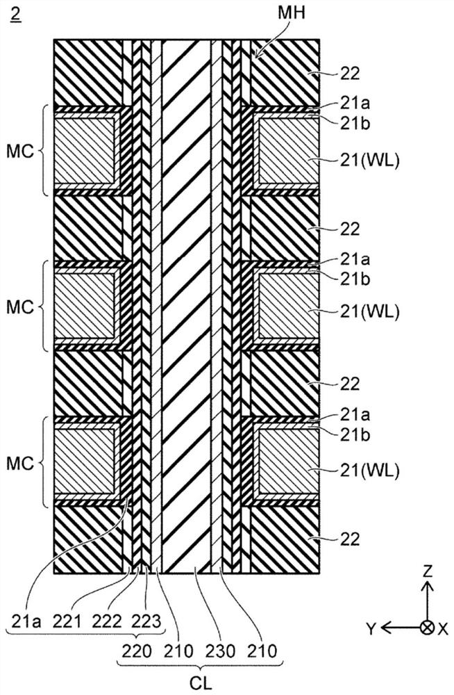
[0023] Figure 1A It is a schematic perspective view illustrating the semiconductor memory device 100a of the first embodiment. Figure 1B It is a schematic plan view showing the laminated body 2 . In this specification, the lamination direction of the laminated body 2 is referred to as the Z direction. One direction intersecting, for example, perpendicular to the Z direction is referred to as the Y direction. One direction intersecting, for example, perpendicular to the Z and Y directions is referred to as the X direction. Figure 2A and Figure 2B Each is a schematic cross-sectional view of a memory cell illustrating a three-dimensional structure. image 3 It is a schematic plan view illustrating the semiconductor memory device 100a of the first embodiment.
[0024] Such as Figure 1A ~ Figure 3 As shown, the semiconductor memory device 100a of the first embodiment is a nonvolatile memory having three-dimensional memory cells.
[0025] The semiconductor memory device 1...
no. 2 Embodiment approach
[0075] Figure 20It is a cross-sectional view showing an example of the configuration of the semiconductor memory device according to the second embodiment. Figure 20 and Figure 5 Similarly, a cross section in a direction perpendicular to the extending direction of the slit SHE when viewed from the lamination direction (Z direction) of the laminate 2 is shown. In the second embodiment, in Figure 20 In the section of , the slit SHE has a middle portion 53 having a width W3 narrower than the width W2 of the bottom thereof. In other words, the slit SHE is wider at the upper opening, but narrows at the middle portion 53, and widens at the bottom. In addition, in the second embodiment, the number of layers of the select gate on the drain side is three layers ( SGD0 to SGD2 ) for convenience.
[0076] The insulating film 50 is filled in the slit SHE from the upper opening to the narrowed middle portion 53 , and has a cavity (void) 51 at the bottom lower than the middle portio...
PUM
 Abstract
Description
Claims
Application Information
 - R&D Engineer
- R&D Manager
- IP Professional
- Industry Leading Data Capabilities
- Powerful AI technology
- Patent DNA Extraction
Browse by: Latest US Patents, China's latest patents, Technical Efficacy Thesaurus, Application Domain, Technology Topic, Popular Technical Reports.
© 2024 PatSnap. All rights reserved.Legal|Privacy policy|Modern Slavery Act Transparency Statement|Sitemap|About US| Contact US: help@patsnap.com