Thin film transistor, preparation method thereof and display substrate

A technology for thin film transistors and a manufacturing method, applied in the field of display substrates, can solve the problems of affecting the normal operation of TFT devices, deteriorating electrical properties of TFT devices, and restoring afterimages. The effect of increasing size or thickness

Active Publication Date: 2021-08-20
WUHAN CHINA STAR OPTOELECTRONICS SEMICON DISPLAY TECH CO LTD
View PDF3 Cites 1 Cited by
  • Summary
  • Abstract
  • Description
  • Claims
  • Application Information

AI Technical Summary

Problems solved by technology

The mobile charge is driven by the current in the TFT device, etc., which will adversely affect the normal operation of the TFT device, thereby deteriorating the electrical performance of the TFT device, and adversely affecting optical evaluation items such as image restoration

Method used


Image

  • Thin film transistor, preparation method thereof and display substrate
  • Thin film transistor, preparation method thereof and display substrate
  • Thin film transistor, preparation method thereof and display substrate

Examples


Embodiment Construction

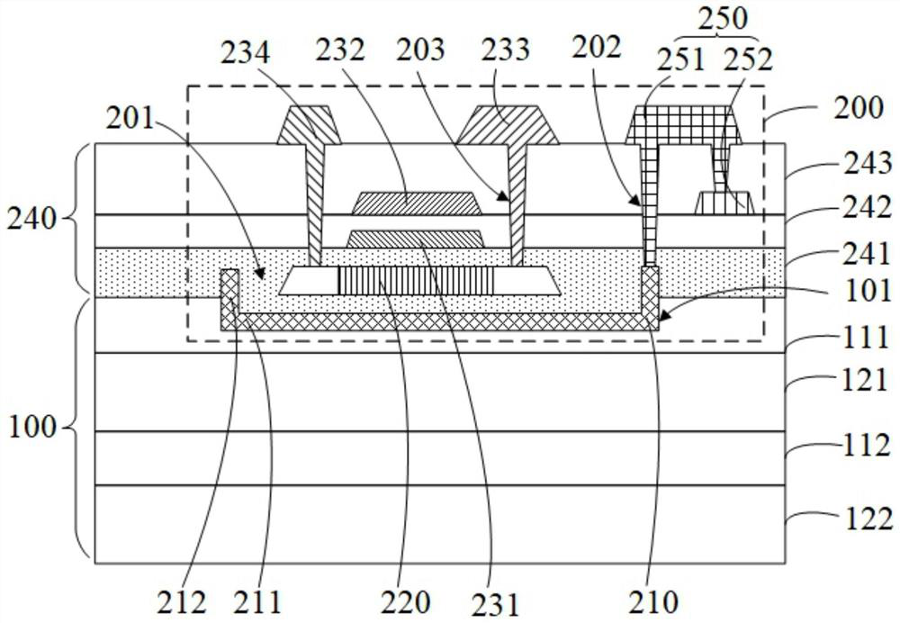
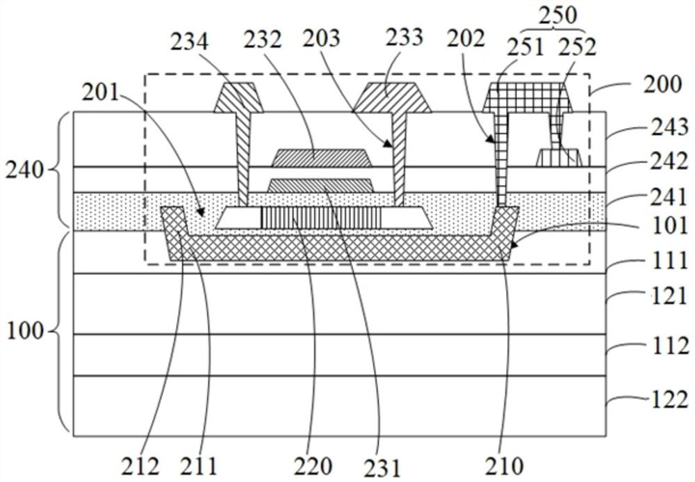
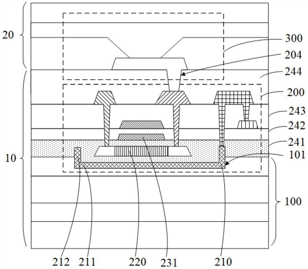
[0043] The technical solutions in the embodiments of the application will be clearly and completely described below in conjunction with the accompanying drawings in the embodiments of the application. Obviously, the described embodiments are only some of the embodiments of the application, not all of them. Based on the embodiments in this application, all other embodiments obtained by those skilled in the art without making creative efforts belong to the scope of protection of this application. In addition, it should be understood that the specific embodiments described here are only used to illustrate and explain the present application, and are not intended to limit the present application. In this application, unless stated to the contrary, the used orientation words such as "up" and "down" usually refer to the up and down of the device in actual use or working state, specifically the direction of the drawings in the drawings ; while "inside" and "outside" refer to the outl...


PUM


Abstract

The embodiment of the invention discloses a thin film transistor, a preparation method thereof and a display substrate. The thin film transistor comprises a shielding structure and an active layer, the shielding structure is provided with a first groove, and a part of or the whole thickness area of the active layer is located in the first groove. According to the thin film transistor, the preparation method thereof and the display substrate, the influence of mobile charges in the organic film layer or the inorganic film layer below or on the side face of the TFT device on the active layer can be shielded through the shielding structure, so that the TFT device keeps excellent electrical characteristics, the problem of residual image restoration is solved, and a flexible display screen with excellent performance is obtained.

Description

technical field [0001] The present application relates to a display substrate, in particular to a thin film transistor, a preparation method, and a display substrate. Background technique [0002] At present, in flexible display screens, there will be certain mobile charges in the organic or inorganic film layer below the Thin Film Transistor (TFT) device. The mobile charge is driven by the current in the TFT device, etc., which will adversely affect the normal operation of the TFT device, thereby deteriorating the electrical performance of the TFT device, and adversely affecting optical evaluation items such as image restoration. [0003] During the research and practice of the prior art, the inventors of the present application discovered an array substrate 10, a manufacturing method, and a display panel to solve the above-mentioned technical problems. Contents of the invention [0004] The embodiment of the present application provides a thin film transistor, its prepa...

Claims


Application Information

Patent Timeline
Patent Type & Authority Applications(China)
IPC IPC(8): H01L29/423H01L29/06H01L29/786H01L21/28H01L21/336G09F9/33
CPCH01L29/78696H01L29/0684H01L29/78609H01L29/66742H01L29/78606H01L29/42384H01L29/42364H01L29/401G09F9/33
Inventor 柯霖波
Owner WUHAN CHINA STAR OPTOELECTRONICS SEMICON DISPLAY TECH CO LTD
Why Eureka
Try Eureka