Gate voltage modulation dynamic source region socket tunneling field effect transistor and preparation method thereof

A technology of tunneling field effect and source region, which is applied in the direction of diodes, semiconductor/solid-state device manufacturing, semiconductor devices, etc., and can solve the problems of carbon nanotube-based graphene-based difficulties, small tunneling probability, and weakening

Active Publication Date: 2021-09-07
JIMEI UNIV
View PDF4 Cites 0 Cited by
  • Summary
  • Abstract
  • Description
  • Claims
  • Application Information

AI Technical Summary

Problems solved by technology

However, both carbon nanotube-based and graphene-based face difficulties in actual fabrication
[0007] Generally speaking, due to the large carrier tunneling quality and forbidden band width of silicon-based TFET, according to the band tunneling probability T WKB It can be seen from the principle that the tunneling probability of TFET devices under the same structure is small, so the on-state current is relatively small, which limits the application of tunneling field effect transistors; and when the TFET device is in the reverse working state, due to the symmetrical structure of the device itself, The "drain-channel" junction will also form a tunnel, which will generate a reverse tunneling current, which is called a bipolar current, which makes the advantage of a small sub-threshold swing weakened by process factors, resulting in a structural performance that cannot meet the requirements.

Method used


Image

  • Gate voltage modulation dynamic source region socket tunneling field effect transistor and preparation method thereof
  • Gate voltage modulation dynamic source region socket tunneling field effect transistor and preparation method thereof
  • Gate voltage modulation dynamic source region socket tunneling field effect transistor and preparation method thereof

Examples


Embodiment Construction

[0055] The present invention will be further described in detail below in conjunction with specific embodiments, which are explanations of the present invention rather than limitations.

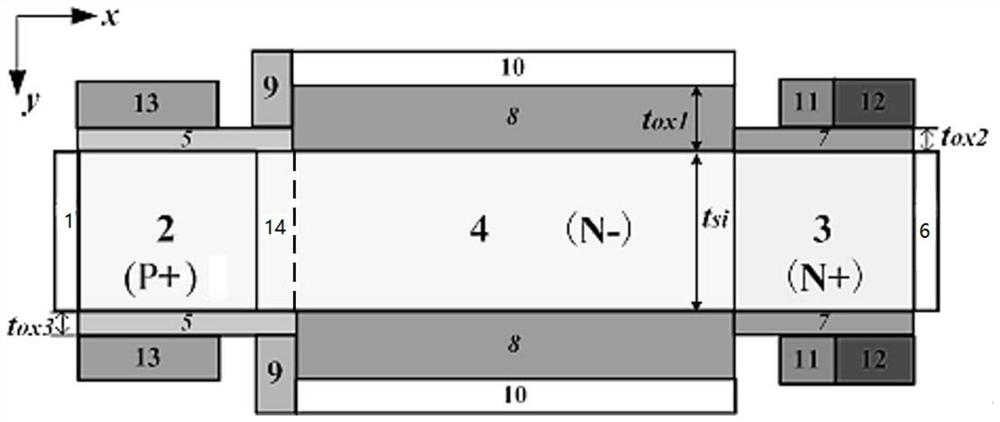
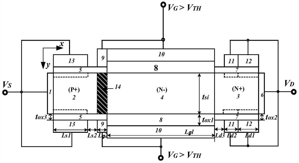
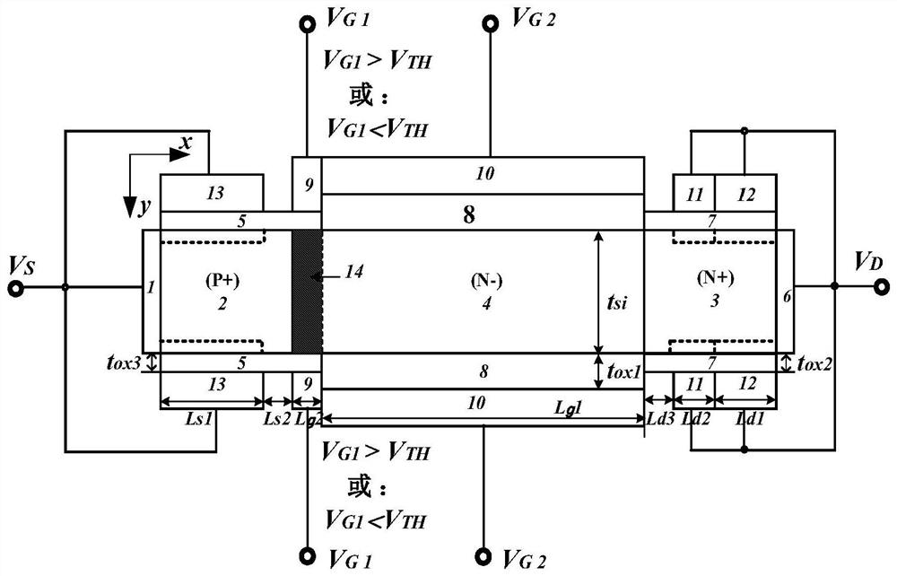
[0056] The invention discloses a tunneling field effect transistor with gate voltage modulation dynamic source region pocket structure and its preparation method. The field effect transistor uses transverse tunneling as the main tunneling mechanism, and the whole is based on longitudinal double-gate ultra-thin body lightly doped tunneling Field effect tube structure (DG-TFET).

[0057] Such as figure 1 As shown, it includes a source region 2, a body region 4 and a drain region 3 arranged in sequence along the lateral direction, and a source region pocket region 14 is formed in the body region 4 close to the interface region of the source region 2; the upper and lower surfaces of the body region 4 are respectively arranged The body region oxide layer 8, the upper and lower surfaces of the bod...


PUM

PropertyMeasurementUnit
widthaaaaaaaaaa
thicknessaaaaaaaaaa
thicknessaaaaaaaaaa

Abstract

The invention provides a gate voltage modulation dynamic source region socket tunneling field effect transistor which is simple in structure, reasonable in design, high in on-state current level and capable of inhibiting generation of bipolar current. The field effect transistor comprises a source region, a body region and a drain region which are sequentially arranged in the transverse direction, wherein a source region socket region is formed in an interface region, close to the source region, in the body region; body region oxide layers are arranged on the upper and lower surfaces of the body region respectively, and main gate polycrystalline silicon electrodes are arranged on the upper and lower surfaces of the body region oxide layers respectively and serve as gate connection gate voltage VGS; the upper and lower surfaces of the source region and the source region socket region are respectively provided with a source region dielectric layer, and the upper and lower surfaces of the source region dielectric layer are respectively provided with a metal gate electrode corresponding to the source region socket region; the metal gate electrode is connected with a gate voltage VGS; drain region oxide layers are respectively arranged on the upper and lower surfaces of the drain region; metal electrodes are arranged on the side faces of the source region and the drain region respectively, serve as a source electrode and a drain electrode and are correspondingly connected with source electrode voltage VS and drain electrode voltage VDS.

Description

technical field [0001] The invention relates to the technical field of semiconductors, in particular to a gate voltage modulation dynamic source region pocket tunneling field effect transistor and a preparation method thereof. Background technique [0002] Tunneling Field Effect Transistor TFET was proposed by H.Kisaki et al. in 1973, and was first applied to CMOS development by P.F.Wang et al. in 2004. In theory, TFET can achieve a sub-threshold swing lower than 60mV / dec, and has the advantages of small off-state current, low static power consumption, and good frequency characteristics. However, the biggest challenge to the applicability of the tunneling field effect transistor is its on-state current (I ON ) 2 to 3 orders of magnitude smaller than MOSFET. [0003] The tunneling field effect transistors in the prior art include the following three types. [0004] The first is a tunneling field effect transistor (All-silicon TFET) using a silicon homojunction. Since the ...

Claims


Application Information

Patent Timeline
Patent Type & Authority Applications(China)
IPC IPC(8): H01L29/08H01L29/417H01L29/423H01L29/43H01L29/739H01L21/28H01L21/331
CPCH01L29/7391H01L29/401H01L29/42312H01L29/41725H01L29/43H01L29/0843H01L29/66356
Inventor 韦素芬李明逵杨证富门凯刘航杨杰圣
Owner JIMEI UNIV
Why Eureka
Try Eureka