
Display module, manufacturing method thereof and display device

A technology for display modules and display segments, which is applied to identification devices, instruments, etc., can solve problems such as the imprint of the adhesive layer on the display module, affecting the appearance of the display module products, etc., to improve the appearance yield, reduce the pressure, increase the The effect of a large pressing area

Active Publication Date: 2021-09-24
WUHAN CHINA STAR OPTOELECTRONICS SEMICON DISPLAY TECH CO LTD
View PDF5 Cites 3 Cited by
  • Summary
  • Abstract
  • Description
  • Claims
  • Application Information

AI Technical Summary

Problems solved by technology

[0005] The present application provides a display module, a manufacturing method thereof, and a display device, which solve the problem of excessive thinning of the buffer layer in order to achieve the effect of a narrow frame in the existing terminal bending process, resulting in obvious imprints of the adhesive layer on the display module and affecting the display module. Technical issues with product appearance

Method used


Image

  • Display module, manufacturing method thereof and display device
  • Display module, manufacturing method thereof and display device
  • Display module, manufacturing method thereof and display device

Examples


Embodiment Construction

[0037] The technical solutions in the embodiments of the present application will be clearly and completely described below in conjunction with the drawings in the embodiments of the present application. Apparently, the described embodiments are only some of the embodiments of this application, not all of them. Based on the embodiments in this application, all other embodiments obtained by those skilled in the art without making creative efforts belong to the scope of protection of this application.

[0038] In the description of the present application, it should be understood that the terms "first" and "second" are used for description purposes only, and cannot be interpreted as indicating or implying relative importance or implicitly indicating the quantity of indicated technical features. Thus, a feature defined as "first" or "second" may explicitly or implicitly include one or more of said features. In the description of the present application, "plurality" means two or ...


PUM


Abstract

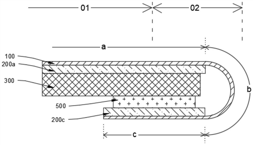
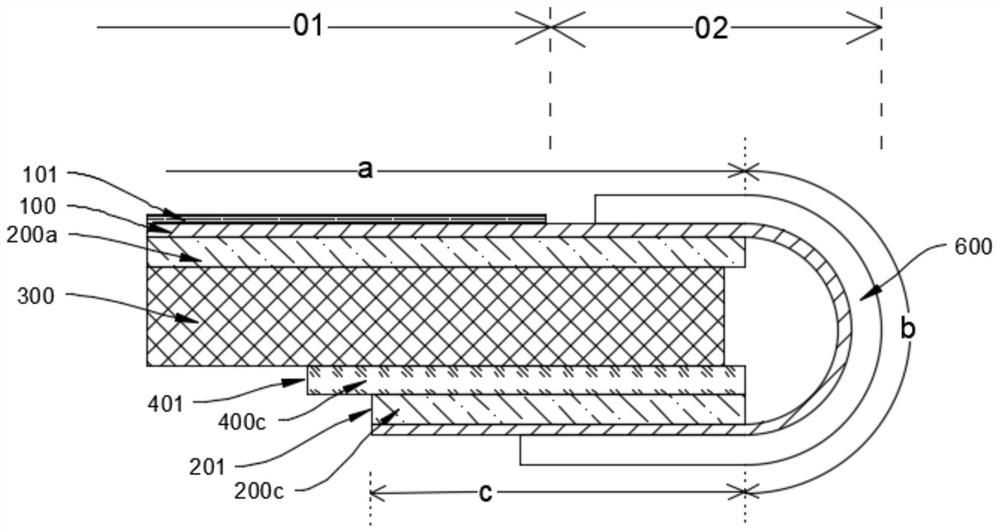
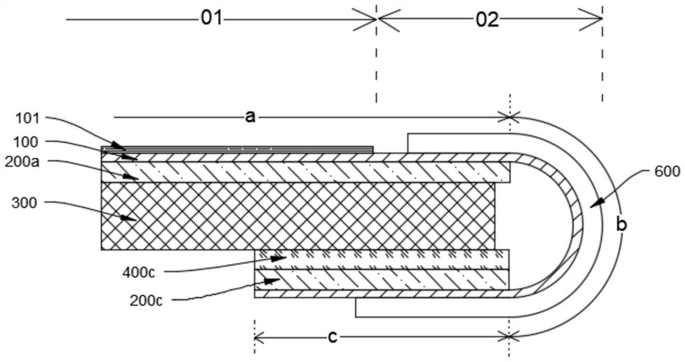
The invention provides a display module, a manufacturing method thereof and a display device. The display module comprises a substrate, a display function layer, a supporting layer, a buffer layer and a first bonding layer. The substrate comprises a display section, a bending section and an extension section; the supporting layer is arranged on one side, far away from the display function layer, of the substrate, and comprises a first supporting layer arranged close to the extension section and a second supporting layer arranged on the display section; the buffer layer is arranged on one side, deviating from the substrate, of the second supporting layer; the first bonding layer is arranged between the first supporting layer and the buffer layer; and the distance from one end, far away from the non-display area, of the first bonding layer to the non-display area is larger than or equal to the distance from one end, far away from the non-display area, of the buffer layer to the non-display area. The technical problem that the appearance of a display module product is affected due to the fact that a buffer layer is excessively thinned in order to achieve a narrow frame effect in an existing terminal bending process, so that a bonding layer on the display module is impressed obviously is solved.

Description

technical field [0001] The present application relates to the field of display modules, in particular to a display module, a manufacturing method thereof, and a display device. Background technique [0002] With the development trend of electronic devices gradually pursuing thinner and narrower borders, due to the constraints of flexible circuit boards (FPC, Flexible Printed Circuit) & line driver array substrates (GOA, Gate driver On Array) and other constraints, the display module's lower The binding at the frame restricts the development of the narrow frame of the mobile phone. [0003] At this stage, the market mainly uses the terminal bending process to bend the FPC&GOA wiring to the back of the screen for binding to achieve the narrow border effect. In order to further reduce the width of the frame, when the terminal bending process of the display module is bound, the minimization of the bending radius is pursued, that is, the thickness of the display module is also r...

Claims


Application Information

Patent Timeline
Patent Type & Authority Applications(China)
IPC IPC(8): G09F9/30
CPCG09F9/301H10K2102/311H10K77/111G06F1/1637G06F1/1652
Inventor 覃黎君
Owner WUHAN CHINA STAR OPTOELECTRONICS SEMICON DISPLAY TECH CO LTD
Learn More