Supercharge Your Innovation With Domain-Expert AI Agents!

Preparation method of semiconductor substrate and semiconductor device

A semiconductor and substrate technology, applied in semiconductor/solid-state device manufacturing, transistors, electrical components, etc., can solve problems such as damage, affecting device performance, and affecting carrier mobility, so as to reduce stress and improve yield.

Active Publication Date: 2021-10-01
CHANGXIN MEMORY TECH INC
View PDF8 Cites 2 Cited by
  • Summary
  • Abstract
  • Description
  • Claims
  • Application Information

AI Technical Summary

Problems solved by technology

This stress usually causes damage to the structure of the semiconductor substrate, such as forming defects or cracks in the active region, or affecting the mobility of carriers in the channel of the device, thereby affecting device performance, etc., and affecting the yield of semiconductor devices

Method used


Image

  • Preparation method of semiconductor substrate and semiconductor device
  • Preparation method of semiconductor substrate and semiconductor device
  • Preparation method of semiconductor substrate and semiconductor device

Examples


Embodiment Construction

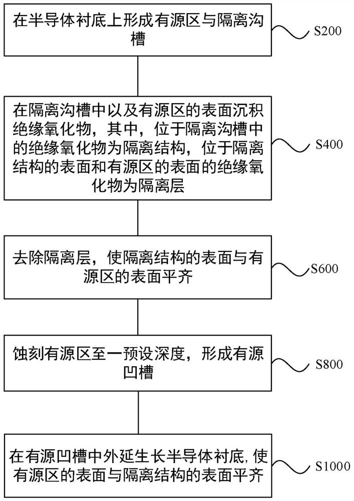
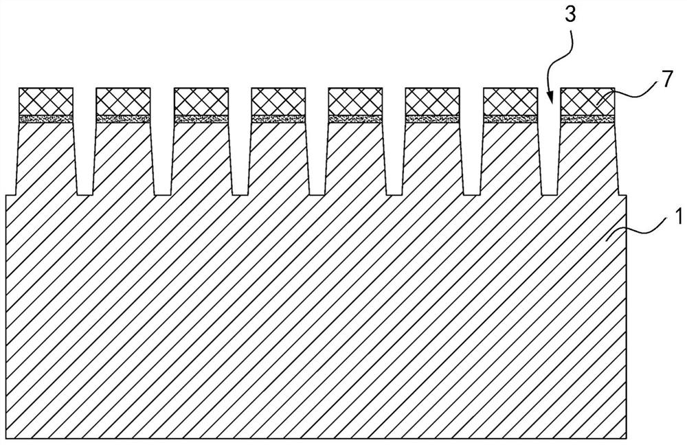
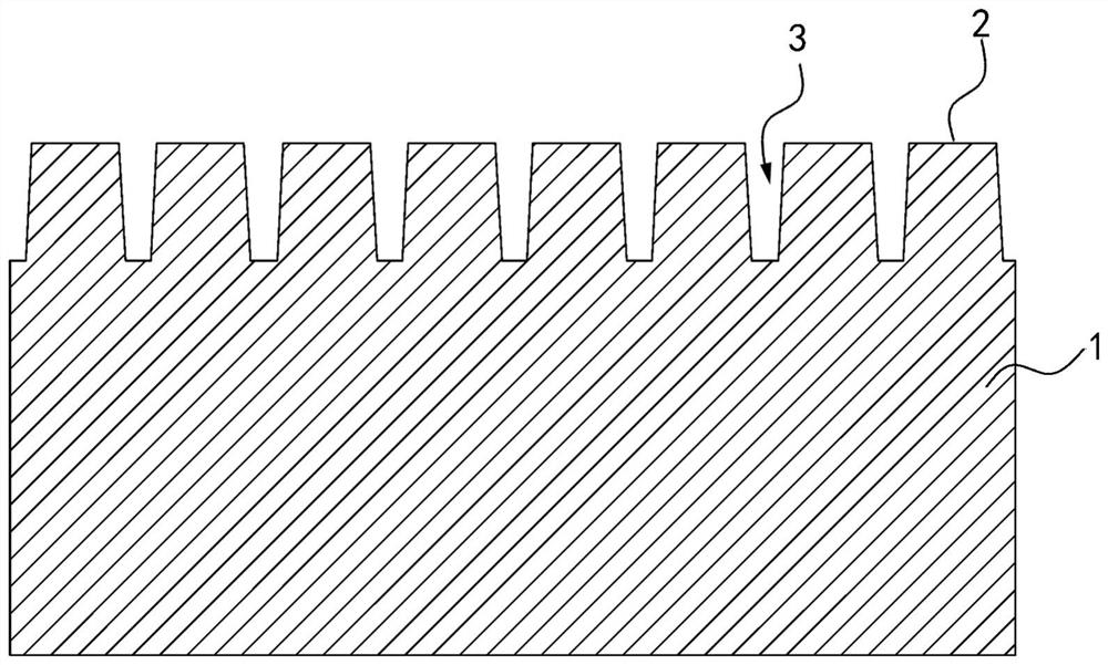
[0036] Example embodiments will now be described more fully with reference to the accompanying drawings. Example embodiments may, however, be embodied in many forms and should not be construed as limited to the embodiments set forth herein; rather, these embodiments are provided so that this disclosure will be thorough and complete, and will fully convey the concept of example embodiments to those skilled in the art. The same reference numerals in the drawings denote the same or similar structures, and thus their detailed descriptions will be omitted.

[0037] In the following description of various exemplary embodiments of the present disclosure, reference is made to the accompanying drawings, which form a part hereof, and in which are shown by way of example different exemplary structures in which aspects of the disclosure may be implemented. It is to be understood that other specific arrangements of components, structures, exemplary devices, systems and steps may be utiliz...


PUM

PropertyMeasurementUnit
thicknessaaaaaaaaaa
thicknessaaaaaaaaaa

Abstract

The invention provides a preparation method of a semiconductor substrate and a semiconductor device. The method comprises the steps of forming an active region and an isolation groove on a semiconductor substrate; depositing insulating oxide in the isolation groove and the surface of the active region, wherein the insulating oxide located in the isolation groove is an isolation structure, and the insulating oxide located on the surface of the isolation structure and the surface of the active region is an isolation layer; removing the isolation layer to enable the surface of the isolation structure to be flush with the surface of the active region; etching the active region to a preset depth to form an active groove; and epitaxially growing a semiconductor substrate in the active groove so as to enable the surface of the active region to be flush with the surface of the isolation structure. According to the preparation method, the stress of the isolation structure and the isolation groove can be eliminated, it is guaranteed that the active region is not damaged by the stress to generate defects or cracks, meanwhile, the mobility of carriers in the channel of the device is prevented from being affected to affect the performance of the device, and the yield of the semiconductor device is improved.

Description

technical field [0001] The invention relates to the technical field of semiconductor manufacturing, in particular to a method for preparing a semiconductor substrate and a semiconductor device. Background technique [0002] During the manufacturing process of semiconductor devices, an active region and an isolation region between the active regions are usually formed in the semiconductor substrate. The formation of the isolation region generally uses a shallow trench isolation process to form a shallow trench, and fills the shallow trench with insulation The material forms shallow trench isolation (STI). [0003] Since the material of the shallow trench isolation is different from the material of the semiconductor substrate, the coefficients of thermal expansion of the two are different, so a certain stress will be generated during the STI process. This stress usually causes damage to the structure of the semiconductor substrate, such as forming defects or cracks in the act...

Claims


Application Information

Patent Timeline
Patent Type & Authority Applications(China)
IPC IPC(8): H01L21/762H01L21/306H01L21/3065H01L27/088
CPCH01L21/76224H01L21/30604H01L21/3065H01L27/088
Inventor 杨航全钟声
Owner CHANGXIN MEMORY TECH INC
Features
  • R&D
  • Intellectual Property
  • Life Sciences
  • Materials
  • Tech Scout
  • Unparalleled Data Quality
  • Higher Quality Content
  • 60% Fewer Hallucinations
Learn More