
A method for producing printed circuit boards

A technology for printed circuit boards and production methods, which is applied in the direction of laminated printed circuit boards, printed circuits, and printed circuit manufacturing. cost, reduction in usage, and production cost savings

Active Publication Date: 2021-11-23
四川英创力电子科技股份有限公司
View PDF0 Cites 0 Cited by
  • Summary
  • Abstract
  • Description
  • Claims
  • Application Information

AI Technical Summary

Problems solved by technology

In the production of the prior art, the core board, the foam board, and the auxiliary frame need to be riveted and bonded together. After the finished area of ​​the printed circuit board is cut, the auxiliary frame will also follow due to the presence of adhesive materials and riveting structures. Scrapped and cannot be reused
When producing this kind of printed circuit board, an auxiliary frame will be scrapped every time one is produced, resulting in a serious waste of resources and increasing the production cost of the circuit board

Method used


Image

  • A method for producing printed circuit boards
  • A method for producing printed circuit boards
  • A method for producing printed circuit boards

Examples


Embodiment 1

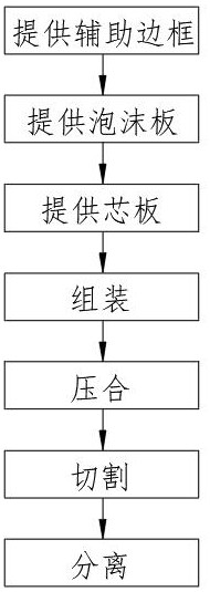
[0044] Such as Figure 1 to Figure 11 Shown, a kind of printed circuit board production method comprises the following steps:

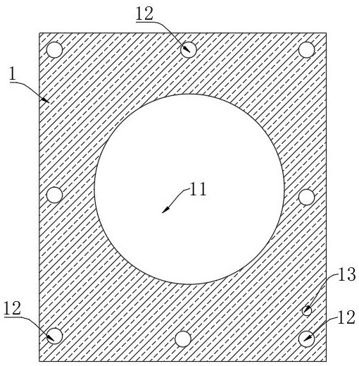
[0045] (1) An auxiliary frame 1 is provided, and a cavity 11 is opened in the middle of the auxiliary frame 1 .

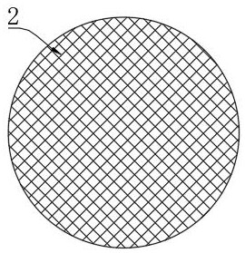
[0046] (2) A foam board 2 is provided, the outer shape of the foam board 2 matches the inner shape of the cavity 11 . In this embodiment, the thickness of the foam board 2 is greater than that of the auxiliary frame 1 .

[0047] (3) A core board 3 is provided. The middle part of the core board 3 has a wiring area 31 , and the range of the wiring area 31 is smaller than the shape range of the foam board 2 .

[0048] (4) Assembling, use the assembly tool to place the foam board 2 in the cavity 11. At this time, there is a gap between the outer wall of the foam board 2 and the inner wall of the cavity 11, so as to facilitate the remaining foam board 2 and auxiliary frame after cutting the finished circuit board 1 separation. In this embod...

Embodiment 2

[0057] Such as Figure 10 As shown, aluminum sheets 5 are provided above the core board 3 and below the auxiliary frame 1 during lamination. The covered area of ​​the aluminum sheet exceeds the edge of the foam board 2 so as to completely cover the wiring area 31 . It can not only protect the wiring area 31 on the surface of the core board 3 , but also prevent the wiring area 31 from being scratched or crushed. At the same time, it also acts as a buffer, which can slow down the contact speed between the pressing plate of the hot pressing device and the core plate 3, so that the pressure is more moderate and uniform, thereby improving the pressing quality.

Embodiment 3

[0059] Such as figure 2 , Figure 4 As shown, the auxiliary frame 1 is provided with a plurality of positioning holes 12 , and the positioning holes 12 are distributed around the cavity 11 at intervals. The core board 3 is provided with pin holes 32 corresponding to the positioning holes 12 .

[0060] When assembling, use the pin shaft 6 to pass through the positioning hole 12 and the corresponding pin hole 32 at the same time. In order to improve the relative position accuracy of the core board 3 and the auxiliary frame 1, and at the same time prevent the relative movement of the core board 3 and the auxiliary frame 1 during pressing.

[0061] preferred, such as Figure 10 As shown, the length of the pin shaft 6 is shorter than the thickness of the laminate assembly, so as to avoid the excessive length of the pin shaft 6 from affecting the thickness of the finished printed circuit board. Because when the length of the pin shaft 6 is greater than the thickness of the lami...


PUM


Abstract

A method for producing a printed circuit board, comprising the steps of: providing an auxiliary frame, and a cavity is formed in the middle of the auxiliary frame; providing a foam board, the outer shape of the foam board coincides with the inner shape of the cavity; providing a core There is a wiring area in the middle of the core board; assembly, place the foam board in the cavity, and there is a gap between the outer wall of the foam board and the inner wall of the cavity; lay an adhesive layer on the top surface of the foam board, and the edge of the adhesive layer is located at the foam within the range of the top surface of the board; lay the core board above the adhesive layer, so that the wiring area is within the range of the adhesive layer; press, press the foam board and the core board to form a composite assembly after pressing; Predetermined trajectory cuts the combined assembly, and forms the finished area of ​​the printed circuit board after cutting; separates the finished area from the combined assembly. The thickness and size of the printed circuit board can be effectively controlled, and the auxiliary frame can be reused to reduce waste of resources and production costs.

Description

technical field [0001] The invention belongs to the technical field of printed circuit board production, and in particular relates to a method for producing a printed circuit board. Background technique [0002] The printed circuit board made of high-frequency circuit core board and foam board is mixed and pressed. The pressure during the lamination process will cause the foam board to become thinner, and eventually the thickness of the printed circuit board will not meet the standard. Therefore, it is necessary to use The board material with high hardness and not easy to be compressed and deformed is used as an auxiliary frame to improve the phenomenon of foam deformation and ensure the final thickness of the printed circuit board. In the production of the prior art, the core board, the foam board, and the auxiliary frame need to be riveted and bonded together. After the finished area of ​​the printed circuit board is cut, the auxiliary frame will also follow due to the pre...

Claims


Application Information

Patent Timeline
Patent Type & Authority Patents(China)
IPC IPC(8): H05K3/00H05K3/38
CPCH05K3/00H05K3/0058H05K3/38
Inventor 李清华牟玉贵张仁军杨海军邓岚
Owner 四川英创力电子科技股份有限公司
Learn More