Image sensor device

An image sensor and substrate technology, applied in the field of image sensors, can solve problems such as crosstalk and sensitivity reduction

Inactive Publication Date: 2021-10-12
SK HYNIX INC
View PDF1 Cites 0 Cited by
  • Summary
  • Abstract
  • Description
  • Claims
  • Application Information

AI Technical Summary

Problems solved by technology

However, incident light may be reflected by the metal wiring layer and may be absorbed by the interlayer insulating film, resulting in reduced sensitivity
In addition, reflected light may be absorbed into adjacent (or adjacent) pixels, causing crosstalk to occur

Method used


Image

  • Image sensor device
  • Image sensor device
  • Image sensor device

Examples


Embodiment Construction

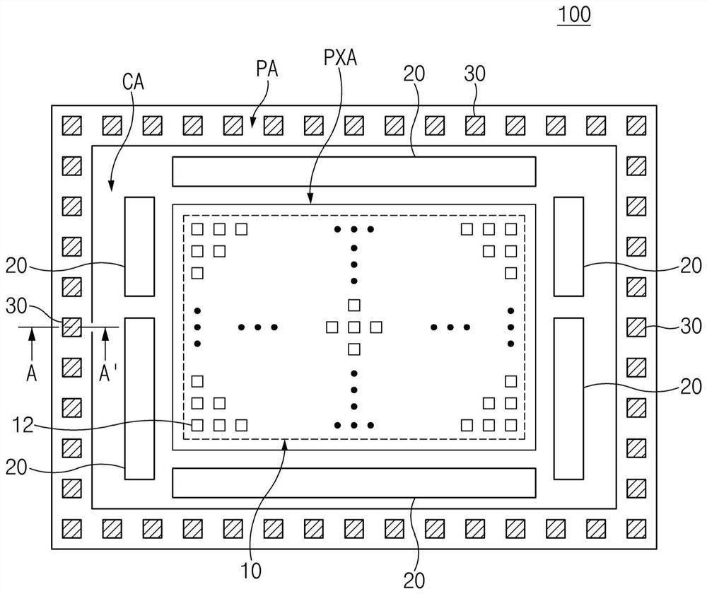
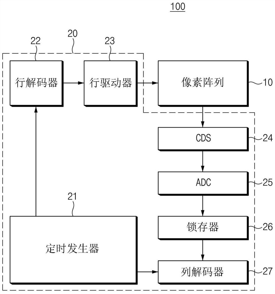
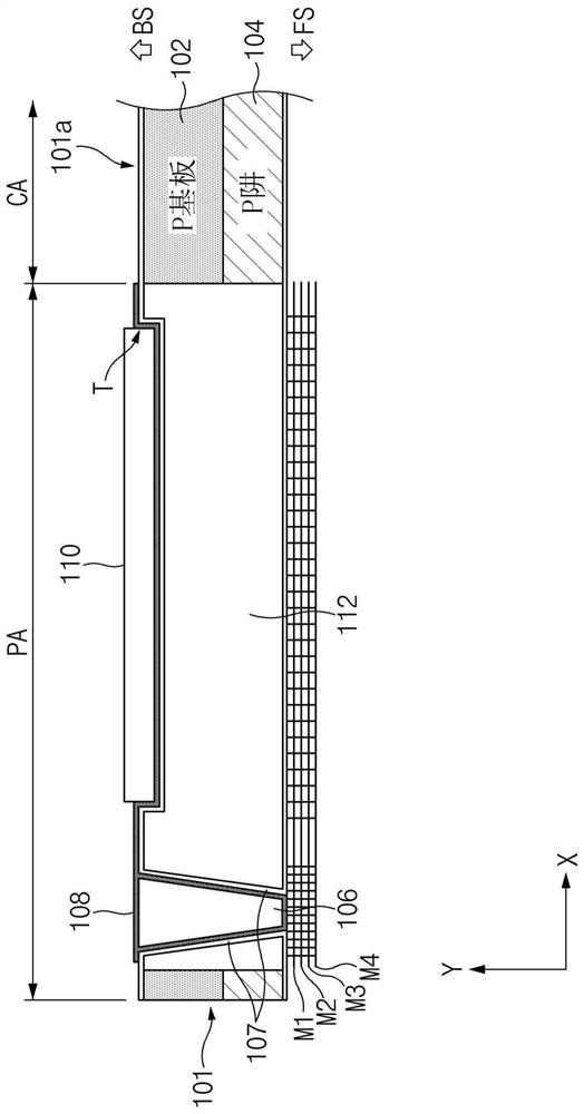
[0019] Various implementations and examples of image sensor devices are provided that address one or more limitations and disadvantages of the related art. Various implementations of the disclosed technology relate to an image sensor device capable of reducing pad area noise and parasitic capacitance and for solving the above-mentioned problems of the prior art.

[0020] Reference will now be made in detail to embodiments of the disclosed technology, examples of which are illustrated in the accompanying drawings. Wherever possible, the same reference numbers will be used throughout the drawings to refer to the same or like parts.

[0021] The advantages and features of the disclosed technology and a method of achieving the advantages and features of the disclosed technology will be clearly understood from the embodiments described below with reference to the accompanying drawings. However, the disclosed technology is not limited to the following embodiments, and can be implem...


PUM


Abstract

An image sensor device is disclosed, which blocks noise of a pad area and minimizes parasitic capacitance of the pad area. The image sensor device includes a substrate including a first surface and a second surface that are arranged to face each other, a pad disposed over the first surface of the substrate, and a noise blocking area formed to overlap with the pad in a first direction, and formed in the substrate.

Description

technical field [0001] The present invention generally relates to image sensor technology, and more particularly, to a technique for blocking noise or minimizing parasitic capacitance of a pad region of an image sensor. Background technique [0002] Image sensors convert optical images into electrical signals. In recent years, due to further research and development in the computer and communication industries, the demand for high-quality, high-performance image sensors has become increasingly popular in various applications such as digital cameras, video cameras, personal communication systems (PCS), game consoles, surveillance cameras, and medical miniature cameras. rapidly growing in many applications and fields. [0003] Specifically, MOS image sensors can be easily driven and implemented using more scanning schemes. The MOS image sensor may include one or more photoelectric conversion elements configured to sense the magnitude of incident light and a multilayer metal ...

Claims


Application Information

Patent Timeline
Patent Type & Authority Applications(China)
IPC IPC(8): H01L27/146
CPCH01L27/14636H01L27/14634H01L27/1464H04N25/616H01L27/14605H01L27/14632H04N25/00H04N25/60
Inventor 李承龙沈亨骏
Owner SK HYNIX INC
Why Eureka
Try Eureka