Display panel, preparation method thereof and display device
A display panel and substrate technology, applied in semiconductor devices, electrical components, circuits, etc., can solve problems such as unevenness of the light-emitting layer, height difference, color shift, etc., to improve height uniformity, improve flatness, and avoid color shift problems Effect
- Summary
- Abstract
- Description
- Claims
- Application Information
AI Technical Summary
Problems solved by technology
Method used
Image
Examples
Embodiment 1
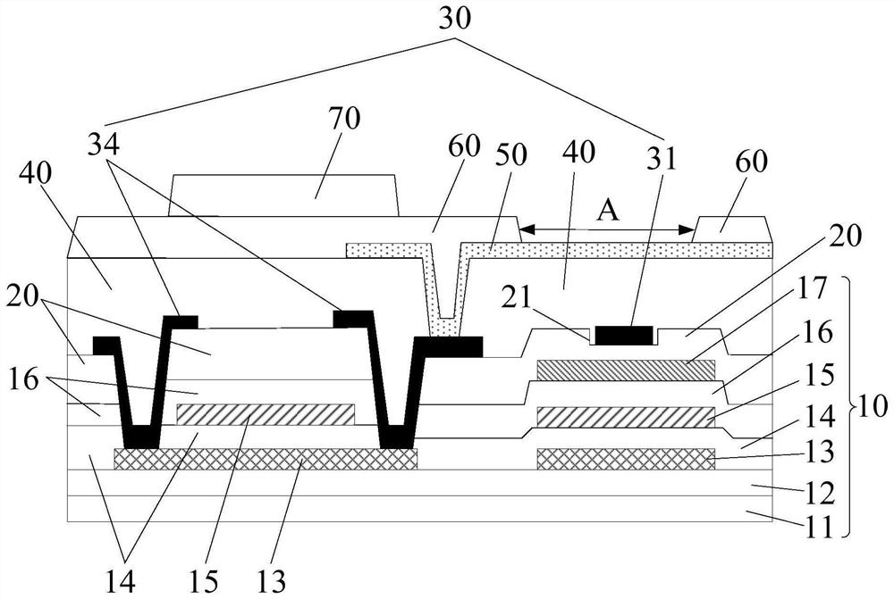
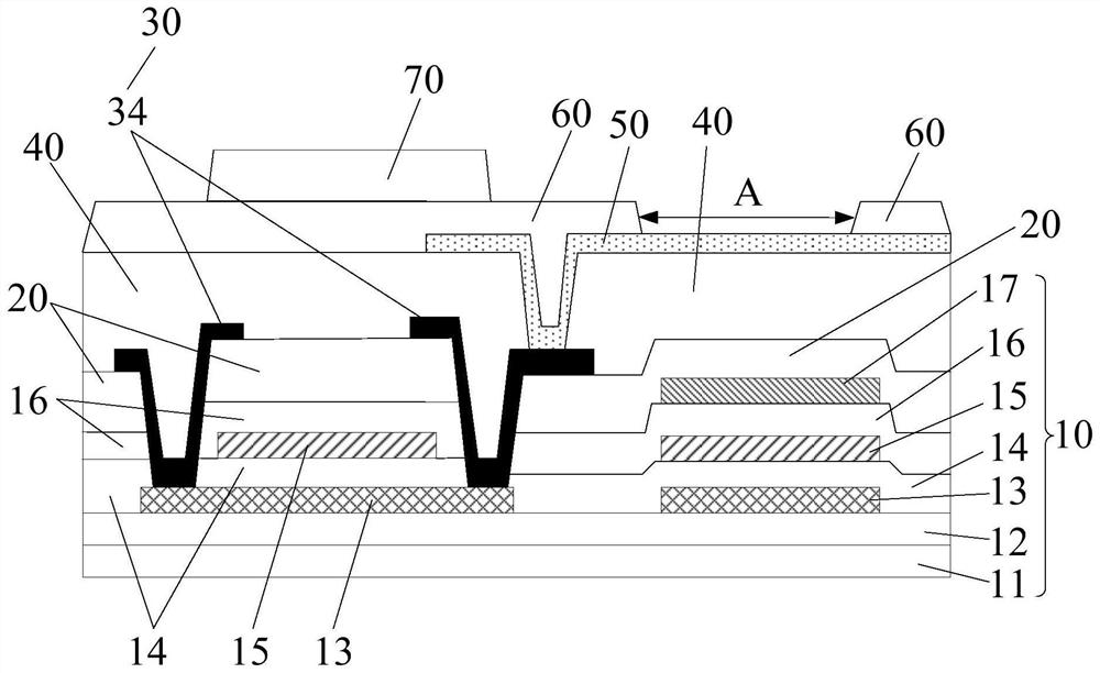
[0055] figure 2 shows a cross-sectional view of a display panel according to Embodiment 1 of the present invention, image 3 shows a cross-sectional view of another display panel according to Embodiment 1 of the present invention, Figure 4 A top view of a display panel according to Embodiment 1 of the present invention is shown. refer to figure 2 and image 3 , the display panel may include a substrate 10, a first insulating layer 20 covering the substrate 10, a wiring layer 30 disposed on the first insulating layer 20, and a second insulating layer covering the wiring layer 30 40, and an anode layer 50 disposed on the second insulating layer 40, the substrate 10 includes a substrate 11, and the display panel includes a pixel opening area A for setting a light emitting device;
[0056] Among them, refer to figure 2 , the wiring layer 30 includes a first wiring portion 31, the orthographic projection of the first wiring portion 31 on the substrate 11 and the orthographic...
Embodiment approach
[0078] For the above first specific implementation manner, since the existing design of the thickness of the first insulating layer can be maintained, there is little change in the manufacturing process of the display panel, which is beneficial to practical use.
[0079] In another optional specific implementation manner, the depth of the groove 21 can also be designed first, and then the thickness of the first insulating layer 20 can be designed to ensure that there will be no defect between the first wiring part 31 and the lower electrode. parasitic capacitance. In this embodiment, the thickness of the first insulating layer 20 can be set thicker than that of the prior art. Specifically, first, the depth of the groove 21 can be designed between 1 / 3-3 / 2 of the thickness of the first wiring part 31, and then the thickness of the first insulating layer 20 between the bottom surface of the groove 21 and the substrate 10 can be designed The thickness is greater than or equal to ...
Embodiment 2
[0088] Figure 5 shows a flow chart of the steps of a method for manufacturing a display panel according to Embodiment 2 of the present invention, Figure 6 A flow chart showing the steps of another method for manufacturing a display panel according to Embodiment 2 of the present invention, refer to Figure 5and Figure 6 , the preparation method comprises the following steps:
[0089] Step 501 : preparing a substrate 10 ; the substrate 10 includes a substrate 11 .
[0090] Optionally, this step may specifically include:
[0091] providing a substrate 11;
[0092] forming a buffer layer 12 on the substrate 11;
[0093] forming an active layer 13 on the buffer layer 12;
[0094] forming a first gate insulating layer 14 covering the active layer 13;
[0095] forming a first gate electrode layer 15 on the first gate insulating layer 14;
[0096] forming a second gate insulating layer 16 covering the first gate electrode layer 15;
[0097] A second gate electrode layer 17...
PUM
 Abstract
Description
Claims
Application Information


