

Test circuit and display panel
A technology for testing circuits and display panels, applied to static indicators, instruments, etc., can solve the problem of affecting the overall width of the lower frame, and achieve the effect of improving stability
- Summary
- Abstract
- Description
- Claims
- Application Information
AI Technical Summary
Problems solved by technology
Method used
Image

Examples
Embodiment Construction
[0023] In order to have a further understanding of the purpose, structure, features and functions of the present invention, the detailed description is as follows in conjunction with the embodiments.
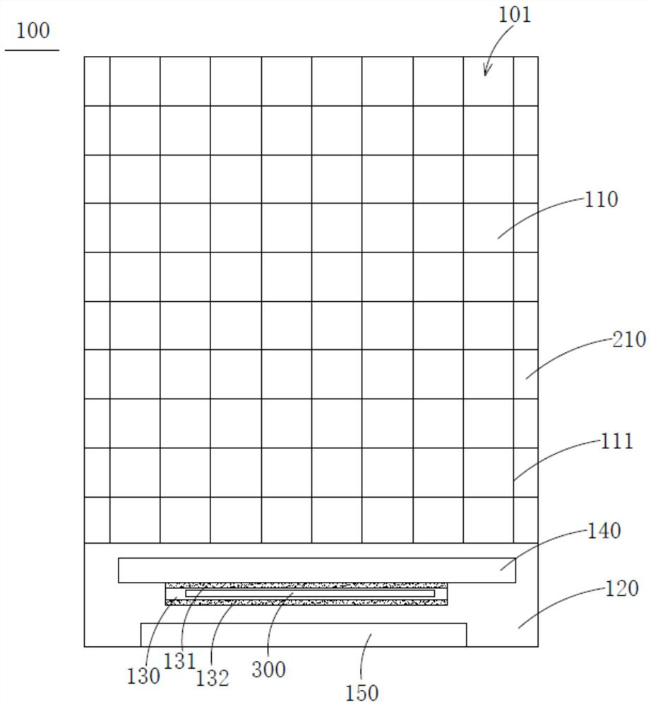
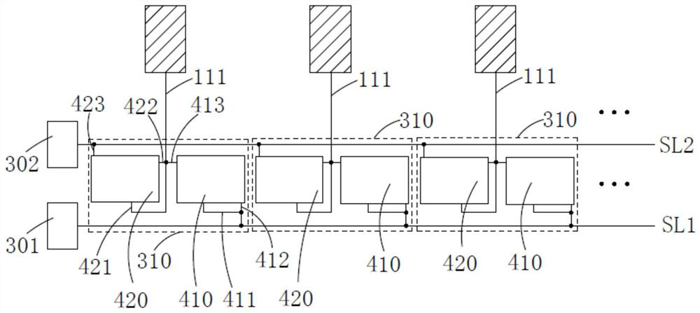
[0024] Please refer to figure 1 , figure 1 is a schematic diagram of the display panel of the present invention, figure 2 It is a schematic diagram of the test circuit of the present invention. Such as figure 1 As shown, the display panel 100 of the present invention has a first substrate 210 , and the first substrate 210 has a display area 110 and a peripheral area 120 . In this embodiment, the display area 110 of the display panel 100 is rectangular. In actual operation, the display panel 100 or the display area 110 can also be set as a circle, ellipse, other irregular arcs, triangles, pentagons or other shapes. polygon. The display area 110 is provided with a plurality of data lines 111 , and a plurality of pixel units 101 are formed into an array and disposed in the di...
PUM
 Abstract
Description
Claims
Application Information