Flip-chip type electro-excitation photonic crystal surface emitting type laser element

一种光子晶体、激光元件的技术,应用在电气元件、激光器零部件、半导体激光器等方向,能够解决散热性差、信号失真、降低激光出光效率等问题,达到提升散热效果、排除寄生电感的效果

Pending Publication Date: 2021-10-29
PHOSERTEK CORP
View PDF5 Cites 0 Cited by
  • Summary
  • Abstract
  • Description
  • Claims
  • Application Information

AI Technical Summary

Problems solved by technology

[0003] However, the first electrode metal and the second electrode metal need to be wire bonded, and wire bonding is a traditional and commonly used packaging technology, which will be accompanied by a strong parasitic inductance effect, which also causes the signal transmission process In this process, serious signal distortion occurs, and the material of the transparent conductive layer is composed of indium tin oxide (Indium Tin Oxide, ITO), which will have optical effects such as absorption, refraction and scattering, thereby reducing the laser light extraction efficiency
In addition, the traditional laser structure has poor heat dissipation, and its performance is more prone to degradation under high current operation

Method used


Image

  • Flip-chip type electro-excitation photonic crystal surface emitting type laser element
  • Flip-chip type electro-excitation photonic crystal surface emitting type laser element
  • Flip-chip type electro-excitation photonic crystal surface emitting type laser element

Examples


Embodiment Construction

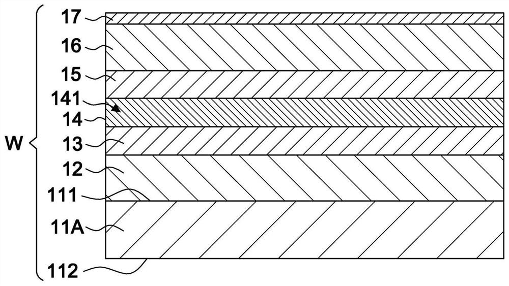
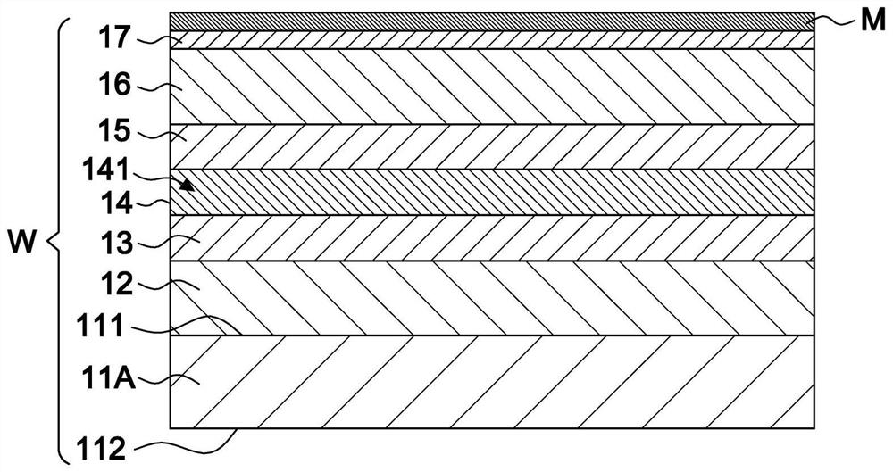
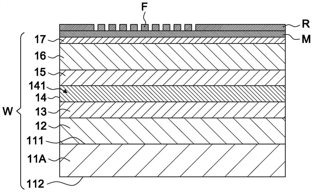
[0032] First, see Figure 1A ~ Figure 1M As shown, a preferred embodiment of a flip-chip electro-excited photonic crystal surface-emitting laser (Electrically Pumped Photonic-Crystal Surface-Emitting Lasers) element 10 of the present invention includes: a first substrate (substrate) 11A, which has A first surface 111 and a second surface 112 on the opposite side. In this embodiment, the material of the first substrate 11A may include gallium nitride (GaN), gallium arsenide (GaAs), indium phosphide (InP ), gallium antimonide (GaSb), but not limited thereto.

[0033]A first cladding layer (cladding layer) 12 is located on the first surface 111 of the first substrate 11A. In this embodiment, the material of the first cladding layer 12 may include aluminum gallium arsenide (AlGaAs ), gallium arsenide (GaAs), aluminum gallium nitride (AlGaN), aluminum gallium indium arsenide (AlGaInAs), aluminum gallium indium phosphide (AlGaInP), aluminum gallium antimonide (AlGaSb), gallium arse...


PUM

PropertyMeasurementUnit
diameteraaaaaaaaaa

Abstract

The invention discloses a flip-chip type electro-excitation photonic crystal surface emitting type laser element. An epitaxial structure of the flip-chip type electro-excitation photonic crystal surface emitting type laser element is provided with a high platform, wherein the high platform is provided with a plurality of air holes to form a photonic crystal structure, the epitaxial structure is also provided with a concave platform, and the facing direction of the concave platform is the same as the facing direction of the photonic crystal structure; a first electrode metal, which is positioned on an insulating layer and covers the photonic crystal structure; and a second electrode metal, which is positioned on the concave platform and protrudes out of the concave platform, so that the facing direction of the first electrode metal and the facing direction of the second electrode metal are the same, and then the first electrode metal is jointed to a first jointing metal and the second electrode metal is jointed to a second jointing metal, so that the photonic crystal structure is flip-chip.

Description

technical field [0001] The invention relates to a flip-chip electro-excited photonic crystal surface-emitting laser element, the first electrode metal and the second electrode metal face the same surface, the first electrode metal can be bonded to the first bonding metal and the second electrode metal can be bonded The second bonding metal makes the photonic crystal structure flip-chip. Background technique [0002] U.S. Patent US10340659B1 discloses an electro-excited photonic crystal surface-emitting laser element, which includes: a substrate with a first surface and a second surface on the opposite side; a first cladding layer located on the first surface of the substrate On the surface; an active layer, located on the first cladding layer, and has a quantum structure; a second cladding layer, located on the active layer; a contact layer, located on the second cladding layer, and with The second cladding layer and the contact layer are in a plateau shape and are provided...

Claims


Application Information

Patent Timeline
Patent Type & Authority Applications(China)
IPC IPC(8): H01S5/042H01S5/024
CPCH01S5/04257H01S5/02476H01S5/02461H01S5/11H01S5/185H01S5/22H01S2301/176H01S5/04252H01S5/04253H01S5/0234H01S5/2027H01S5/04256H01S5/34346H01S5/18H01S5/2209H01S5/0206
Inventor 陈俞谌周柏存林建宏翁志源
Owner PHOSERTEK CORP
Why Eureka
Try Eureka