Development debugging system, to-be-tested device and debugging method

A technology for equipment under test and debugging system, which is applied in software testing/debugging, error detection/correction, instruments, etc. It can solve the problems of PCB space and IC pins occupying too much, and solve the problem of PCB space and IC pins occupying too much many effects

Pending Publication Date: 2021-11-09
芯来智融半导体科技(上海)有限公司
View PDF5 Cites 1 Cited by
  • Summary
  • Abstract
  • Description
  • Claims
  • Application Information

AI Technical Summary

Problems solved by technology

[0008] In the embodiment of the present application, a development and debugging system, a device under test and a debugging method are provided. By multiplexing the debugging interface and the reset interface, the problem of excessive occupation of PCB space and IC pins is solved.

Method used


Image

  • Development debugging system, to-be-tested device and debugging method
  • Development debugging system, to-be-tested device and debugging method
  • Development debugging system, to-be-tested device and debugging method

Examples


Embodiment Construction

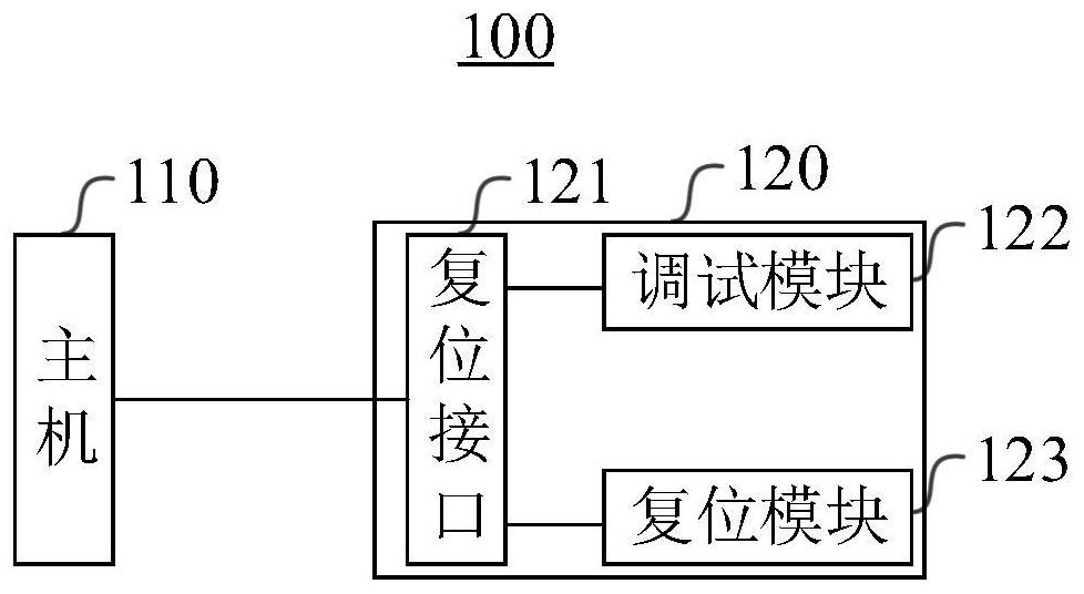
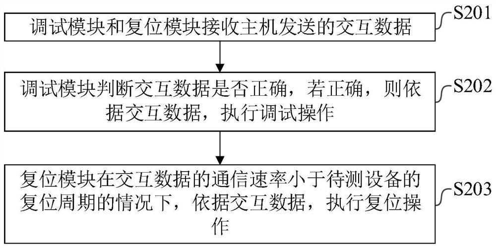
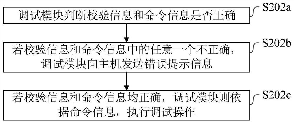
[0027] In the process of implementing the present application, the inventors found that the current debugging interface is set separately and not multiplexed with other functions, and there is a problem that PCB space and IC pins are too much occupied.

[0028] In view of the above problems, the embodiment of the present application provides a development and debugging system, a device under test and a debugging method. By setting the communication rate of interactive data, the debugging signal and the reset signal can be distinguished, and then the debugging interface and the reset interface can be realized. Multiplexing, no need to set up a separate debugging interface, which solves the problem of excessive PCB space and IC pin occupation.

[0029] The solutions in the embodiments of the present application can be realized by using various computer languages, for example, the object-oriented programming language Java and the literal translation scripting language JavaScript. ...


PUM


Abstract

The embodiment of the invention provides a development debugging system, a to-be-tested device and a debugging method. The development debugging system comprises a host and the to-be-tested device. The to-be-tested device comprises a reset interface, a debugging module and a reset module, and the host is connected with the debugging module and the reset module through the reset interface; the host is used for sending interaction data to the debugging module and the reset module through the reset interface; the debugging module is used for judging whether the interaction data is correct or not, and if yes, debugging operation is executed according to the interaction data; and the reset module is used for executing reset operation according to the interaction data under the condition that the communication rate of the interaction data is smaller than the reset period of the to-be-tested equipment. By setting the communication rate of the interactive data, the debugging signal and the reset signal can be distinguished, so that multiplexing of the debugging interface and the reset interface can be realized, the debugging interface does not need to be independently arranged, and the problem that the PCB space and the IC pin occupy too much is solved.

Description

technical field [0001] The present application relates to the technical field of debugging, and in particular, relates to a development and debugging system, a device under test and a debugging method. Background technique [0002] Usually the debugging interface solution used in the industry is the standard JTAG (Joint Test Action Group, Joint Test Working Group) boundary scan interface, and the JTAG boundary scan interface includes at least 4 input and output lines: test clock, test mode, test data input and test data output . Since it needs to occupy at least 4 debugging signal lines, it becomes more and more difficult to realize under the condition that PCB (Printed Circuit Board, printed circuit board) space and IC (integrated circuit, integrated circuit) pins are increasingly scarce due to the miniaturization of electronic products. [0003] Although the industry already has a small size debugging protocol set 1149.7 (IEEE Standard for Reduced-Pin and Enhanced-Functio...

Claims


Application Information

Patent Timeline
Patent Type & Authority Applications(China)
IPC IPC(8): G06F11/36
CPCG06F11/3656
Inventor 万瑞罡
Owner 芯来智融半导体科技(上海)有限公司
Why Eureka
Try Eureka