Substrate bonding device, substrate bonding method, and electronic device manufacturing method

A technology for laminating devices and substrates, which is applied in semiconductor/solid-state device manufacturing, electronic equipment, chemical instruments and methods, etc., can solve the problems of substrate handling deterioration and achieve the effect of reducing the number of residues and warping

Pending Publication Date: 2021-11-16
ASAHI GLASS CO LTD
View PDF7 Cites 0 Cited by
  • Summary
  • Abstract
  • Description
  • Claims
  • Application Information

AI Technical Summary

Problems solved by technology

[0004] However, when the thickness of the substrate becomes thinner, the handleability of the substrate deteriorates, so it is difficult to form functional layers for electronic devices (Thin Film Transistor (TFT: Thin Film Transistor), color filter (CF: ColorFilter)) on the surface of the substrate

Method used


Image

  • Substrate bonding device, substrate bonding method, and electronic device manufacturing method
  • Substrate bonding device, substrate bonding method, and electronic device manufacturing method
  • Substrate bonding device, substrate bonding method, and electronic device manufacturing method

Examples


Embodiment Construction

[0041] Embodiments of the present invention will be described below with reference to the drawings.

[0042] Hereinafter, the case where the bonding apparatus and bonding method of the board|substrate of this invention are used in the manufacturing process of an electronic device is demonstrated.

[0043] Electronic devices refer to electronic components such as display panels, solar cells, and thin-film secondary batteries. Examples of the display panel include a liquid crystal display panel (LCD: Liquid Crystal Display), a plasma display panel (PDP: Plasma Display Panel), and an organic EL display panel (OELD: Organic Electro Luminescence Display).

[0044] Manufacturing process of electronic devices

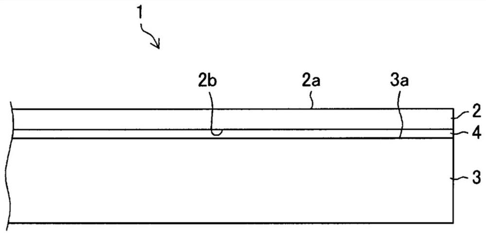
[0045] Electronic devices are produced by forming functional layers for electronic devices (thin-film transistors (TFTs) and color filters (CFs) in the case of LCDs) on surfaces of substrates made of glass, resin, or metal.

[0046] Before forming the functional layer, the...


PUM


Abstract

The invention provides a substrate bonding device, a substrate bonding method, and an electronic device manufacturing method. A first substrate and a second substrate are bonded to each other with an adhesive layer therebetween. A first roller presses the second substrate against the first substrate while the second substrate is subjected to bending deformation and, while rolling, the first roller applies the entire surface of the second substrate to the first substrate by means of a first force. A second roller, while rolling, applies a second force that is greater than the first force to the laminated body formed by the application of the entire surface of the second substrate to the first substrate, thereby pressure bonding the entire surface of the second substrate to the first substrate.

Description

[0001] This application has an international application date of November 19, 2015 (date of entering the Chinese national phase: April 13, 2017), an international application number of PCT / JP2015 / 082556 (national application number: 201580055520.5), and an invention title of "Substrate The laminating device and laminating method and the manufacturing method of the electronic device" is a divisional application. technical field [0002] The present invention relates to a bonding device and bonding method of substrates and a manufacturing method of electronic devices. Background technique [0003] With thinner and lighter electronic devices such as display panels, solar cells, and thin-film secondary batteries, thinner substrates (first substrates) such as glass plates, resin plates, and metal plates used in these electronic devices are expected. [0004] However, when the thickness of the substrate becomes thinner, the handleability of the substrate deteriorates, so it is dif...

Claims


Application Information

Patent Timeline
Patent Type & Authority Applications(China)
IPC IPC(8): H01L21/683H01L21/67B32B37/00B32B37/10
CPCB32B7/06B32B37/10B29C63/02G02F1/13G02F1/1333H01L21/683B32B37/003B32B37/0053H01L21/185H01L21/67092B32B2457/00
Inventor 宇津木洋伊藤泰则大坪豊
Owner ASAHI GLASS CO LTD
Why Eureka
Try Eureka