A kind of diode and its manufacturing method

A manufacturing method and diode technology, applied in semiconductor/solid-state device manufacturing, semiconductor devices, electrical components, etc., can solve the problems of excessive pulse voltage and large energy loss at the moment of turn-on, so as to speed up turn-on speed and reduce the impact of withstand voltage , the effect of strong pressure resistance

Active Publication Date: 2022-03-15
杭州芯逐半导体有限公司
View PDF0 Cites 0 Cited by
  • Summary
  • Abstract
  • Description
  • Claims
  • Application Information

AI Technical Summary

Problems solved by technology

This is because the device will accumulate charges in the inversion-doped region in the blocking state, and in the process of switching to the on-state, the charges in the floating inversion-doped region are restricted by the electric field and cannot be released, so they cannot be released in the blocking state. Normal opening under low pressure
This turn-on recovery problem causes floating junction devices to cause excessive pulse voltage at the moment of turn-on in circuit applications, resulting in excessive energy loss

Method used


Image

  • A kind of diode and its manufacturing method
  • A kind of diode and its manufacturing method
  • A kind of diode and its manufacturing method

Examples


Embodiment 1

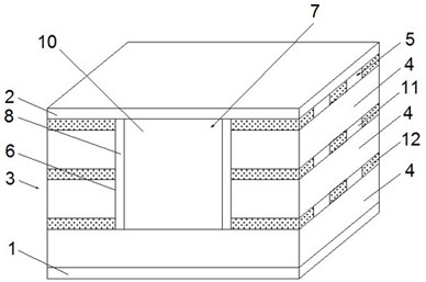
[0033] like figure 1 As shown, a diode includes a cathode layer 1, an anode layer 2 and a diode body 3. The diode body 3 includes more than two groups of substrate layers 4 and more than two groups of intermediate layers 5, and a A group of intermediate layers 5, or a group of substrate layers 4 is arranged between every two groups of intermediate layers 5, and the numbers of the substrate layers 4 and the intermediate layers 5 can be the same or different. When the numbers of the substrate layers 4 and the intermediate layers 5 are different, The difference between the two numbers is one, and more than one set of trenches 6 are opened on the diode body 3 , and the trenches 6 run through all the intermediate layers 5 , and the sidewalls of the trenches 6 are provided with connection layers 7 .

[0034] In this embodiment, the substrate layer 4 is used as the first layer, and the combination is carried out in such a way that the intermediate layer 5 and the substrate layer 4 ar...

Embodiment 2

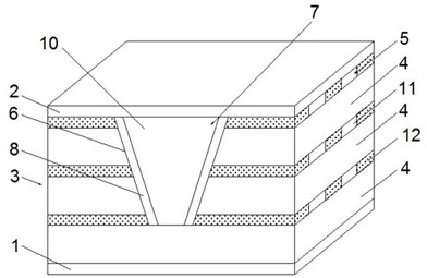
[0042] like figure 2 As shown, a diode includes a cathode layer 1, an anode layer 2 and a diode body 3. The diode body 3 includes more than two groups of substrate layers 4 and more than two groups of intermediate layers 5, and a A group of intermediate layers 5, or a group of substrate layers 4 is arranged between every two groups of intermediate layers 5, and the numbers of the substrate layers 4 and the intermediate layers 5 can be the same or different. When the numbers of the substrate layers 4 and the intermediate layers 5 are different, The difference between the two numbers is one, and more than one set of trenches 6 are opened on the diode body 3 , and the trenches 6 run through all the intermediate layers 5 , and the sidewalls of the trenches 6 are provided with connection layers 7 .

[0043] In this embodiment, the substrate layer 4 is used as the first layer, and the combination is carried out in such a way that the intermediate layer 5 and the substrate layer 4 a...

Embodiment 3

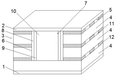
[0052] like image 3 As shown, the connection layer 7 includes a first semiconductor layer 8, a second semiconductor layer 9 and an insulating filling layer 10, the first semiconductor layer 8 is disposed on the sidewall of the trench 6, and the second semiconductor layer 9 is disposed on the first semiconductor layer 8 is away from the side wall of the trench 6, the insulating filling layer 10 is arranged between the second semiconductor layer 9, the plane where the side wall of the trench 6 is located is perpendicular to the plane where the middle layer 5 is located, and the first semiconductor layer 8 and the middle layer Layer 5 is of the same type of semiconductor material, and the second semiconductor layer 9 is of the same type of semiconductor material as substrate layer 4 .

[0053] like Figure 5 As shown, the intermediate layer 5 includes an epitaxial layer 11 and a doped layer 12, wherein the epitaxial layer 11 is an N-type semiconductor material having the same d...


PUM

PropertyMeasurementUnit
angleaaaaaaaaaa

Abstract

The invention relates to a diode in the technical field of semiconductors and a manufacturing method thereof, comprising a cathode layer, an anode layer and a diode body. The diode body includes more than two groups of substrate layers and more than two groups of intermediate layers. A group of intermediate layers is provided, or a group of substrate layers is provided between every two groups of intermediate layers, and more than one group of grooves are opened on the diode body, and the grooves run through all the intermediate layers, and a connecting layer is arranged on the side walls of the grooves. It has the advantage of improving the withstand voltage, and breaks through the bottleneck that the diode affects the normal turn-on speed under low voltage.

Description

technical field [0001] The invention relates to the technical field of semiconductors, in particular to a diode and a manufacturing method thereof. Background technique [0002] In recent years, more and more attention has been paid to energy saving and emission reduction in the world, which puts forward higher requirements for loss control and efficiency improvement of large power electronic equipment. As an important part of power electronic equipment, semiconductor power devices have received extensive attention from the industry. [0003] Breakdown voltage is an important indicator of semiconductor power devices, indicating the maximum voltage that the device can withstand. The active region of the power device can obtain a breakdown voltage of several thousand volts through the introduction of multi-layer inversion doped regions, which is suitable for higher power applications. This kind of semiconductor device that introduces multiple layers of inversion doped region...

Claims


Application Information

Patent Timeline
Patent Type & Authority Patents(China)
IPC IPC(8): H01L29/861H01L29/06H01L21/329
CPCH01L29/861H01L29/0619H01L29/6609
Inventor 盛况王珩宇王策
Owner 杭州芯逐半导体有限公司
Why Eureka
Try Eureka