Opening speed improved superhigh-voltage silicon carbide thyristor and manufacturing method thereof

A technology of silicon carbide crystal and silicon carbide, which is applied in semiconductor/solid-state device manufacturing, electrical components, circuits, etc., can solve the problems of limited improvement of turn-on time, increase the complexity of test circuits, etc., and achieve the effect of increased turn-on speed

Inactive Publication Date: 2019-05-31
XIAN UNIV OF TECH
View PDF2 Cites 8 Cited by
  • Summary
  • Abstract
  • Description
  • Claims
  • Application Information

AI Technical Summary

Problems solved by technology

However, the above methods have limited improvement on the turn-on time and will increase the complexity of the test circuit and other issues

Method used


Image

  • Opening speed improved superhigh-voltage silicon carbide thyristor and manufacturing method thereof
  • Opening speed improved superhigh-voltage silicon carbide thyristor and manufacturing method thereof
  • Opening speed improved superhigh-voltage silicon carbide thyristor and manufacturing method thereof

Examples


Embodiment 1

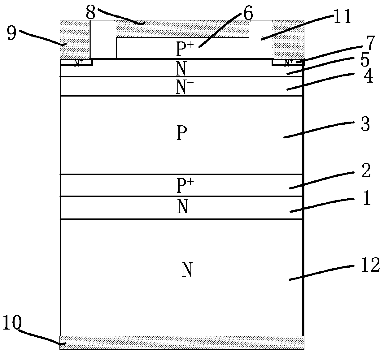
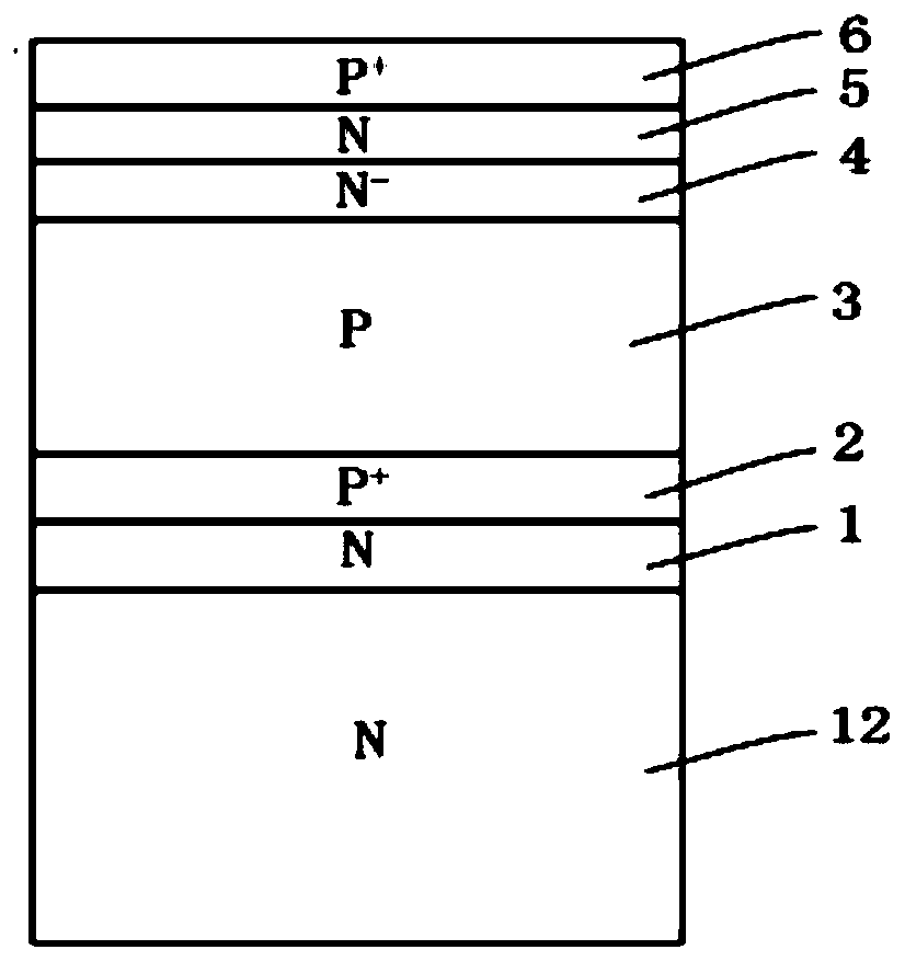
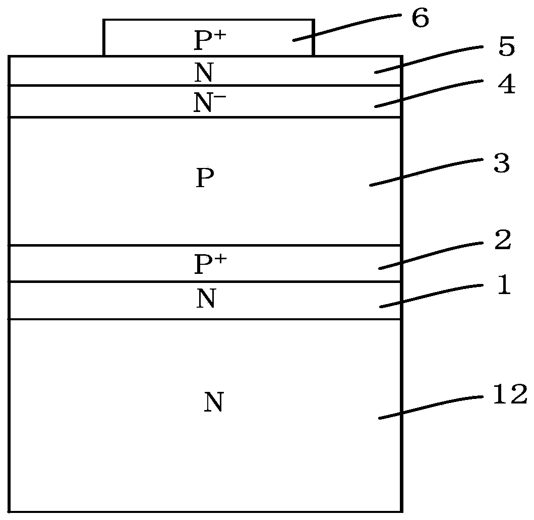
[0061] Step 1. First select a 4H-SiC single crystal substrate, and then epitaxially grow silicon carbide N buffer layer 1, silicon carbide P+ buffer layer 2, silicon carbide P long base region 3, and silicon carbide N- low-doped silicon carbide substrate on the substrate surface. Region 4, silicon carbide N highly doped region 5 and silicon carbide P+ emitter region 6, the thickness of the 4H-SiC single crystal substrate is 300-350 μm;

[0062] The doping concentration of silicon carbide N buffer layer 1 is 2x10 18 cm -3 , the thickness of SiC N buffer layer 1 is 1.0 μm, and the doping concentration of SiC P+ buffer layer 2 is 2x10 17 cm -3 , the thickness of the silicon carbide P+ buffer layer 2 is 2.0 μm, and the doping concentration of the silicon carbide P long base region 3 is 2×10 14 cm -3 , the thickness of the silicon carbide P long base region 3 is 160 μm, and the doping concentration of the silicon carbide N-lowly doped region 4 is 2×10 14 cm -3 , the thickness o...

Embodiment 2

[0071] Step 1. First select a 6H-SiC single crystal substrate, and then epitaxially grow silicon carbide N buffer layer 1, silicon carbide P+ buffer layer 2, silicon carbide P long base region 3, and silicon carbide N- low-doped silicon carbide substrate on the substrate surface. Region 4, silicon carbide N highly doped region 5 and silicon carbide P+ emitter region 6, the thickness of the 4H-SiC single crystal substrate is 320 μm;

[0072] The doping concentration of silicon carbide N buffer layer 1 is 2x10 18 cm -3 , the thickness of SiC N buffer layer 1 is 1.0 μm, and the doping concentration of SiC P+ buffer layer 2 is 2.5x10 17 cm -3 , the thickness of the silicon carbide P+ buffer layer 2 is 2.2 μm, and the doping concentration of the silicon carbide P long base region 3 is 2.x10 14 cm -3 , the thickness of the silicon carbide P long base region 3 is 161 μm, and the doping concentration of the silicon carbide N-lowly doped region 4 is 2.5×10 14 cm -3 , the thicknes...

Embodiment 3

[0081] Step 1. First select a 4H-SiC single crystal substrate, and then epitaxially grow silicon carbide N buffer layer 1, silicon carbide P+ buffer layer 2, silicon carbide P long base region 3, and silicon carbide N- low-doped silicon carbide substrate on the substrate surface. Region 4, silicon carbide N highly doped region 5 and silicon carbide P+ emitter region 6, the thickness of the 4H-SiC single crystal substrate is 330 μm;

[0082] The doping concentration of silicon carbide N buffer layer 1 is 3x10 18 cm -3 , the thickness of SiC N buffer layer 1 is 1.2 μm, and the doping concentration of SiC P+ buffer layer 2 is 3x10 17 cm -3 , the thickness of the silicon carbide P+ buffer layer 2 is 2.5 μm, and the doping concentration of the silicon carbide P long base region 3 is 1.4×10 14 cm -3 , the thickness of the silicon carbide P long base region 3 is 163 μm, and the doping concentration of the silicon carbide N-lowly doped region 4 is 3×10 14 cm -3 , the thickness o...


PUM

PropertyMeasurementUnit
thicknessaaaaaaaaaa
thicknessaaaaaaaaaa
thicknessaaaaaaaaaa

Abstract

The invention discloses an opening speed improved superhigh-voltage silicon carbide thyristor which comprises an N+ type silicon carbide substrate, and a silicon carbide N buffer layer, a silicon carbide P+ buffer layer, a silicon carbide P long base region, a silicon carbide N- lowly doped region, a silicon carbide N highly doped region and a silicon carbide P+ emitter region in epitaxial growthon the upper surface of the N+ type silicon carbide substrate successively, the silicon carbide P+ emitter region is positioned on the silicon carbide N highly doped region, the surface of the siliconcarbide P+ emitter region is covered with an anode Ohmic electrode in a contact way, silicon carbide heavily doped N+ areas are embedded into the upper of the two ends of the silicon carbide N highlydoped region respectively, the surface of each silicon carbide heavily doped N+ area is covered with a gate Ohmic electrode, a gate-anode isolated region is formed between each gate Ohmic electrode and the silicon carbide P+ emitter region, and the backside of the N+ type silicon carbide substrate is covered with a cathode Ohmic electrode. The invention also discloses a preparation method of thethyristor. The opening speed of the thyristor is improved.

Description

technical field [0001] The invention belongs to the technical field of semiconductor electronics and electric power, and relates to an ultra-high-voltage silicon carbide thyristor with improved turn-on speed, and also relates to a preparation method of the ultra-high-voltage silicon carbide thyristor with improved turn-on speed. Background technique [0002] For a long time, silicon thyristors have been in a monopoly position in UHVDC systems, but their voltage blocking ability, switching speed, and dv / dt and di / dt resistance have gradually approached what silicon materials can achieve. Physical limits, and can not work in high temperature (greater than 125 ℃) environment, therefore, we need to find new semiconductor materials to meet the development needs of power electronic devices. [0003] Silicon carbide (4H-SiC), as a relatively mature third-generation wide-bandgap semiconductor material, has a wider bandgap than silicon, about three times that of silicon; a higher bre...

Claims


Application Information

Patent Timeline
Patent Type & Authority Applications(China)
IPC IPC(8): H01L29/10H01L29/744H01L21/332
Inventor 蒲红斌刘青王曦安丽琪
Owner XIAN UNIV OF TECH
Why Eureka
Try Eureka