Thyristor gate cathode structure and gate pole commutation thyristor with thyristor gate cathode structure

A gate cathode and thyristor technology, which is applied in the field of semiconductor device structure, can solve the problem of high doping concentration, and achieve the effects of increasing on-current, increasing turn-on speed and improving turn-on speed.

Active Publication Date: 2013-07-24
ZHUZHOU CRRC TIMES SEMICON CO LTD
View PDF5 Cites 8 Cited by
  • Summary
  • Abstract
  • Description
  • Claims
  • Application Information

AI Technical Summary

Problems solved by technology

[0010] attached by image 3 It can be seen that although the gate-cathode junction structure in the prior art and the thyristor with this structure have a large amount of electron injection from the N+ emitter region 6, due to the high doping concentration of the P+ short base region 5, a large amount of electrons are provided. The holes, where the electrons recombine with the holes, thus reducing the amount of electron injection in the P-base and N-base regions, which becomes a factor limiting the conductance modulation effect

Method used


Image

  • Thyristor gate cathode structure and gate pole commutation thyristor with thyristor gate cathode structure
  • Thyristor gate cathode structure and gate pole commutation thyristor with thyristor gate cathode structure
  • Thyristor gate cathode structure and gate pole commutation thyristor with thyristor gate cathode structure

Examples


Embodiment 1

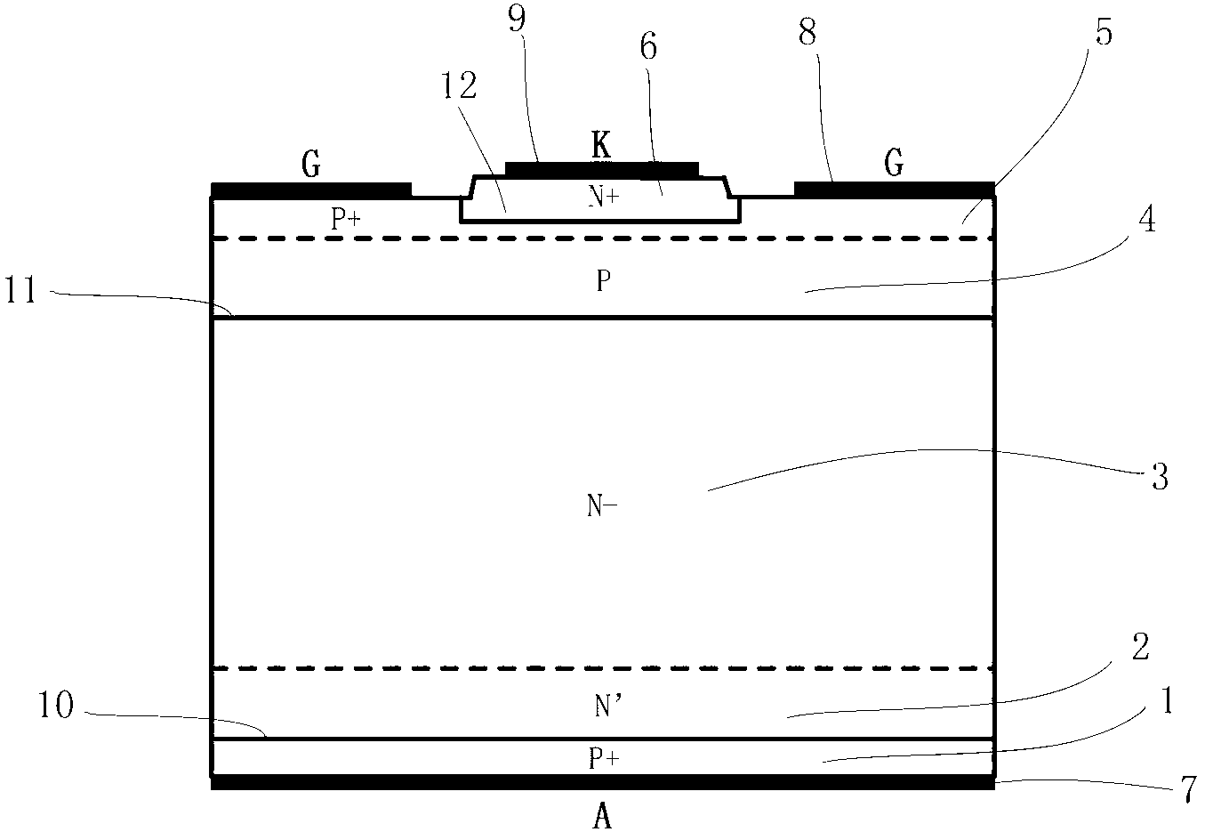
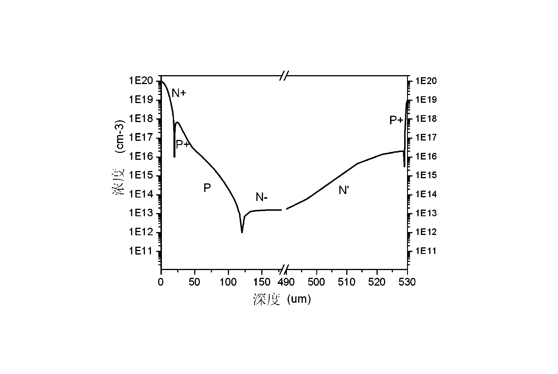
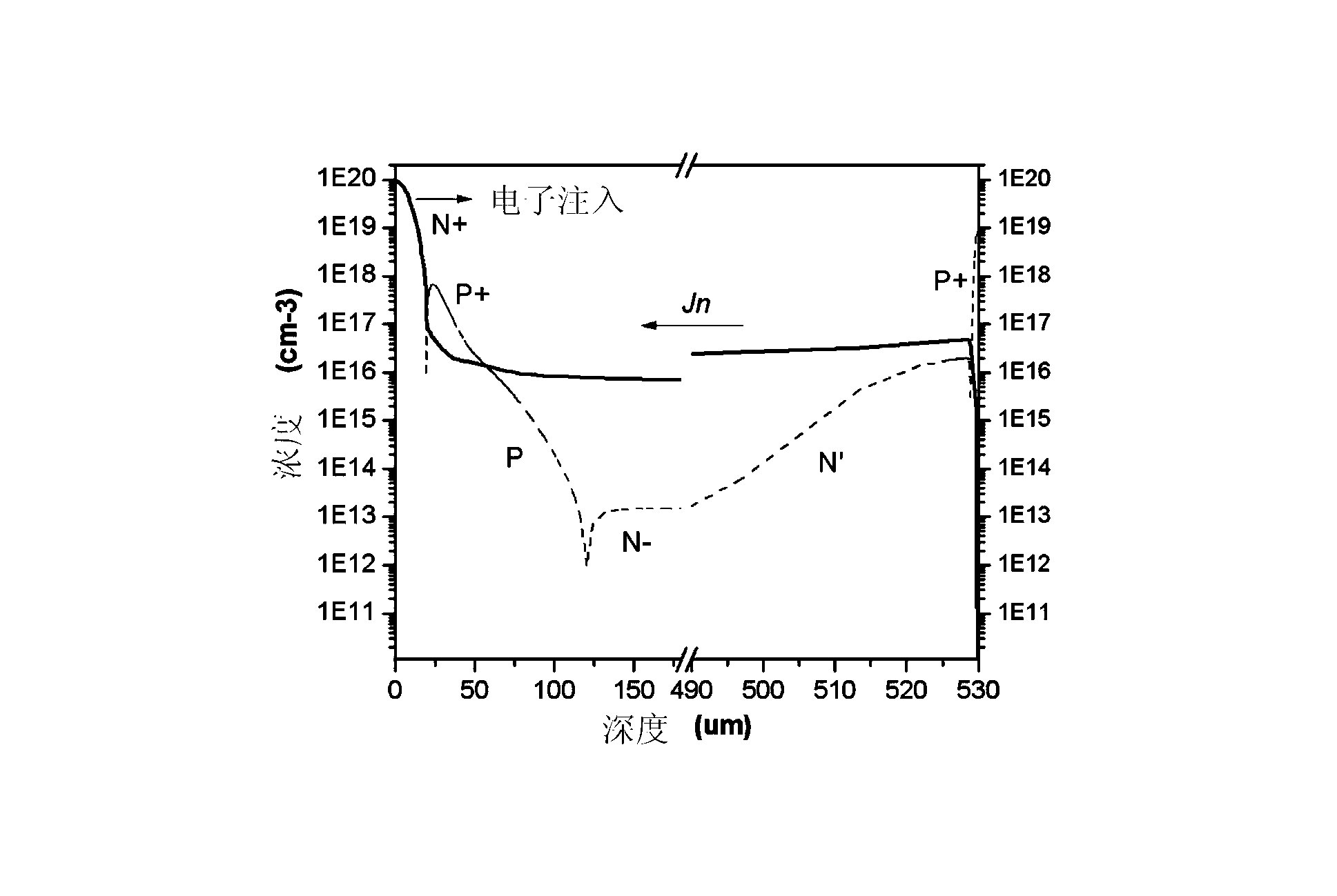
[0113] as attached Figure 43 A specific implementation method of a gate-commutated thyristor manufacturing method shown in the process of A. The gate-commutated thyristor includes more than one cell, and the manufacturing method of the gate-commutated thyristor includes more than one gate-commutated thyristor cell. The preparation method, wherein, the preparation method of a single gate commutated thyristor cell comprises the following steps:

[0114] S101: Prepare N-type substrate, as attached Figure 22 shown;

[0115] S102: Perform selective P+ diffusion treatment on the front side of the N-type substrate to form a P+ short base region 5, as shown in the attached Figure 23 As shown in the figure, the width L between the two P+ short base regions 5 is adjustable;

[0116] S103: Perform P diffusion treatment on the front side of the N-type substrate to form the P base region 4, and form the J2 junction 11 between the P base region 4 and the N-substrate 3, as shown in the...

Embodiment 2

[0127] as attached Figure 43 A specific implementation method of a gate-commutated thyristor manufacturing method shown in the process of C. The gate-commutated thyristor includes more than one cell, and the manufacturing method of the gate-commutated thyristor includes more than one gate-commutated thyristor cell. The preparation method, the preparation method of a single gate commutated thyristor cell comprises the following steps:

[0128] S301: preparing an N-type substrate;

[0129] S302: Perform P diffusion treatment on the front side of the N-type substrate to form a P base region 4, and form a J2 junction 11 between the P base region 4 and the N-substrate 3;

[0130] S303: performing selective P+ diffusion treatment on the front side of the N-type substrate to form a P+ short base region 5;

[0131] S304: performing N' diffusion treatment on the back surface of the N-type substrate to form an N' buffer layer 2;

[0132] S305: performing N+ pre-deposition treatment ...

Embodiment 3

[0143] as attached Figure 43 A specific implementation method of a gate-commutated thyristor manufacturing method shown in the process of B, the gate-commutated thyristor includes more than one cell, and the manufacturing method of the gate-commutated thyristor includes more than one gate-commutated thyristor cell The preparation method, the preparation method of a single gate commutated thyristor cell comprises the following steps:

[0144] S201: Prepare N-type substrate, as attached Figure 32 shown;

[0145] S202: Perform P' diffusion treatment on the front side of the N-type substrate, as shown in the attached Figure 33 shown;

[0146] S203: Perform selective P+ diffusion treatment on the front side of the N-type substrate to form a P+ short base region 5, as shown in the attached Figure 34 shown;

[0147] S204: Perform P diffusion treatment on the front side of the N-type substrate to form the P base region 4, and form the J2 junction 11 between the P base region ...


PUM


Abstract

The invention discloses a thyristor gate cathode structure and a gate pole commutation thyristor with the thyristor gate cathode structure. The thyristor comprises an N-substrate, a P base region, a P+ short base region, an N+ emitter region, a door pole metal electrode and a cathode metal electrode. The N+ emitter region, the P+ short base region, the P base region and the N-substrate are sequentially distributed, the cathode metal electrode is arranged on the outer surface of the N+ emitter region, and the door pole metal electrode is arranged on the outer surface of the P+ short base region. The thyristor gate cathode structure is of a two-layer step structure, wherein the first layer of steps is a shallow step, and the bottom of the first layer of the steps is a P+N+ boundary. The second layer of the steps is a deep step, and the bottom of the second layer of the steps is a PN+ boundary. The gate pole commutation thyristor with the thyristor gate cathode structure further comprises an N' buffer layer and a P+ anode region. The combination of electrons injected in the N+ emitter region of the thyristor is reduced at the P+ short base region and the P base region, conductivity modulation effects of the thyristor are intensified, and connected currents and the starting speed can be further improved.

Description

technical field [0001] The invention relates to a semiconductor device structure, in particular to a thyristor gate-cathode junction structure applied in the field of power semiconductors, and a gate-commutated thyristor having the gate-cathode junction. Background technique [0002] Silicon is a kind of semiconductor material. The semiconductor devices represented by silicon are all processed on the basis of the original single crystal. By doping a small amount of impurities into it, the conductivity is significantly changed, thereby forming a specific structure and doping. Miscellaneous distribution, so as to realize the function of the device. The dopants are divided into two categories: one is N-type dopants, such as phosphorus and arsenic atoms. The other type is P-type dopants, such as boron, aluminum and gallium atoms. Doping phosphorus, arsenic, and antimony can make silicon an electron-conducting type (N-type) silicon, and doping boron, aluminum or gallium can mak...

Claims


Application Information

Patent Timeline
Patent Type & Authority Applications(China)
IPC IPC(8): H01L29/74H01L29/06H01L29/08
Inventor 唐龙谷冯江华吴煜东陈勇民陈芳林
Owner ZHUZHOU CRRC TIMES SEMICON CO LTD
Why Eureka
Try Eureka