Semiconductor Device, RFID Tag Using the Same and Display Device

a technology of rfid tag and semiconductor device, which is applied in the direction of semiconductor device, electrical apparatus, transistor, etc., can solve the problems of difficult to reduce standby power consumption, difficult to produce a fully depleted state, and difficult to operate at a low voltage of about 1 to 3 v, so as to achieve high field effect mobility and high on-current

Inactive Publication Date: 2013-04-25
HITACHI LTD
View PDF2 Cites 34 Cited by
  • Summary
  • Abstract
  • Description
  • Claims
  • Application Information

AI Technical Summary

Benefits of technology

[0020]The following is a brief description of the advantageous effects achieved by the representative elements of the invention laid open in this application.
[0021]A semiconductor device having a thin-film transistor which provides a sub-threshold slope of 100 mV / decade, a high on-current and a high field effect mobility can be realized.

Problems solved by technology

However, a thin-film transistor which uses a silicon-based semiconductor material has a problem that its sub-threshold slope is as large as about 200 mV / decade and if this thin-film transistor is used to form a circuit, operation at a low voltage of about 1 to 3 V, at which an ordinary large-scale integrated circuit operates, is difficult.
In addition, since its off-current is large, it has a problem that it is difficult to decrease the standby power consumption.
A solution to these problems is to produce a fully depleted state while the thin-film transistor is off, but in the case of a thin-film transistor which uses a silicon-based semiconductor material, for a reason related to the manufacturing process, it is not easy to produce a fully depleted state.

Method used


Image

  • Semiconductor Device, RFID Tag Using the Same and Display Device
  • Semiconductor Device, RFID Tag Using the Same and Display Device
  • Semiconductor Device, RFID Tag Using the Same and Display Device

Examples


first embodiment

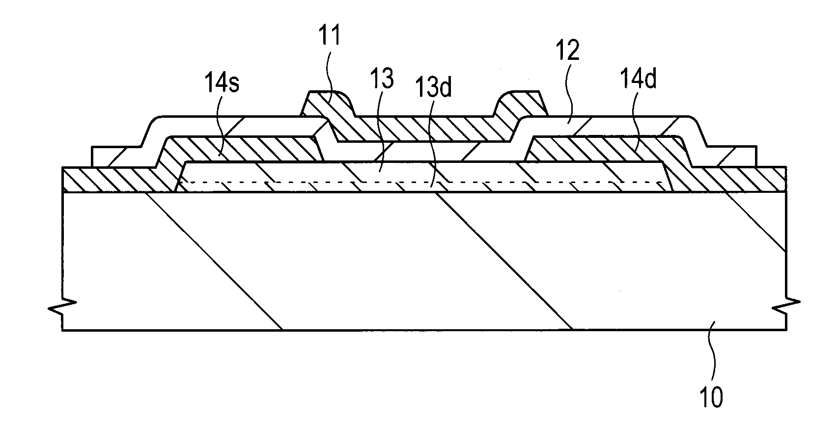
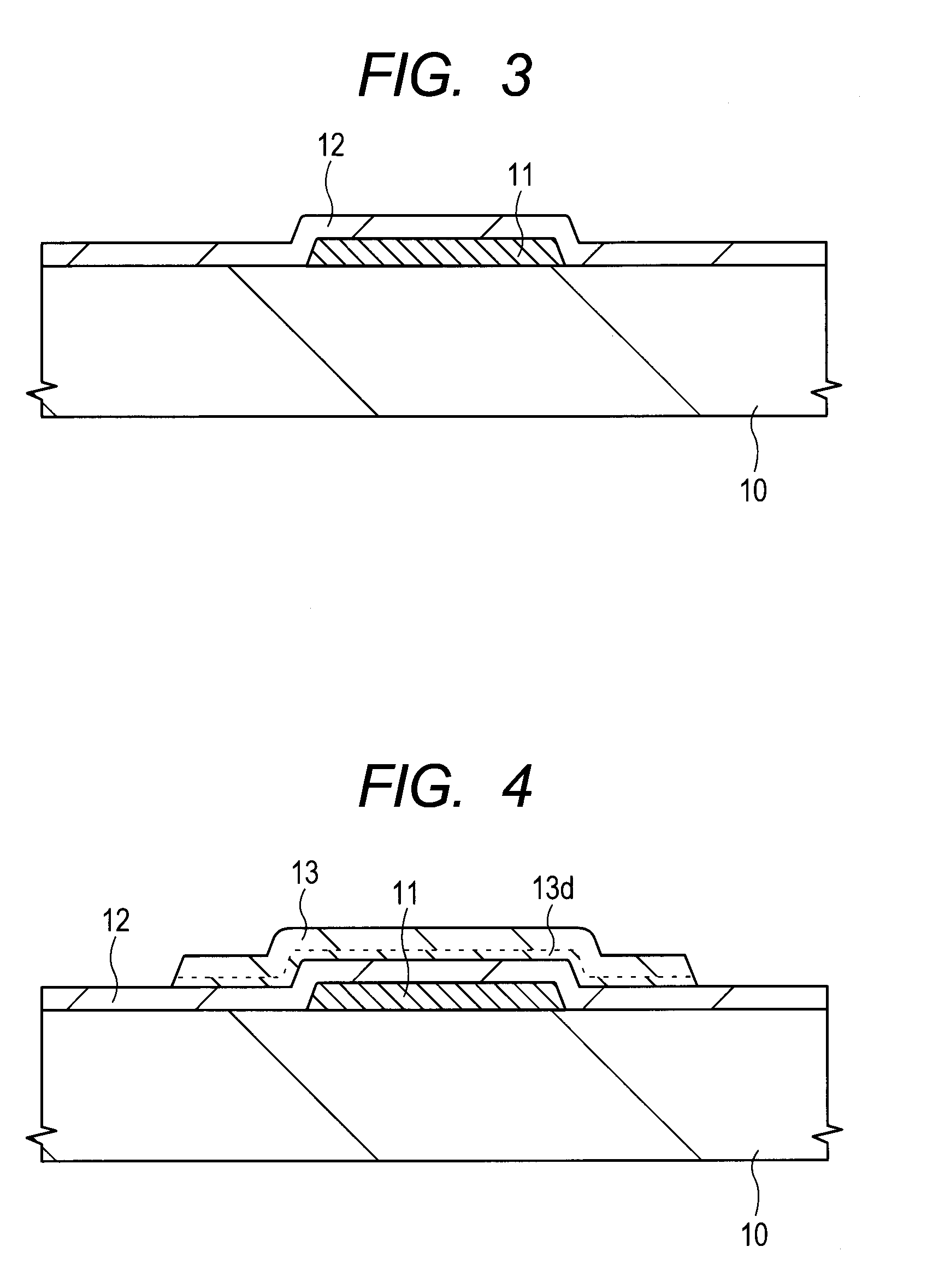
[0046]The first embodiment is applied to a bottom gate / top contact thin-film transistor. Here, “bottom gate” means a structure in which a gate electrode is located in a layer under a channel layer and “top contact” means a structure in which a source electrode and a drain electrode are located in a layer above a channel layer. Next, the method of manufacturing a bottom gate / top contact thin-film transistor will be described in the order of process steps.

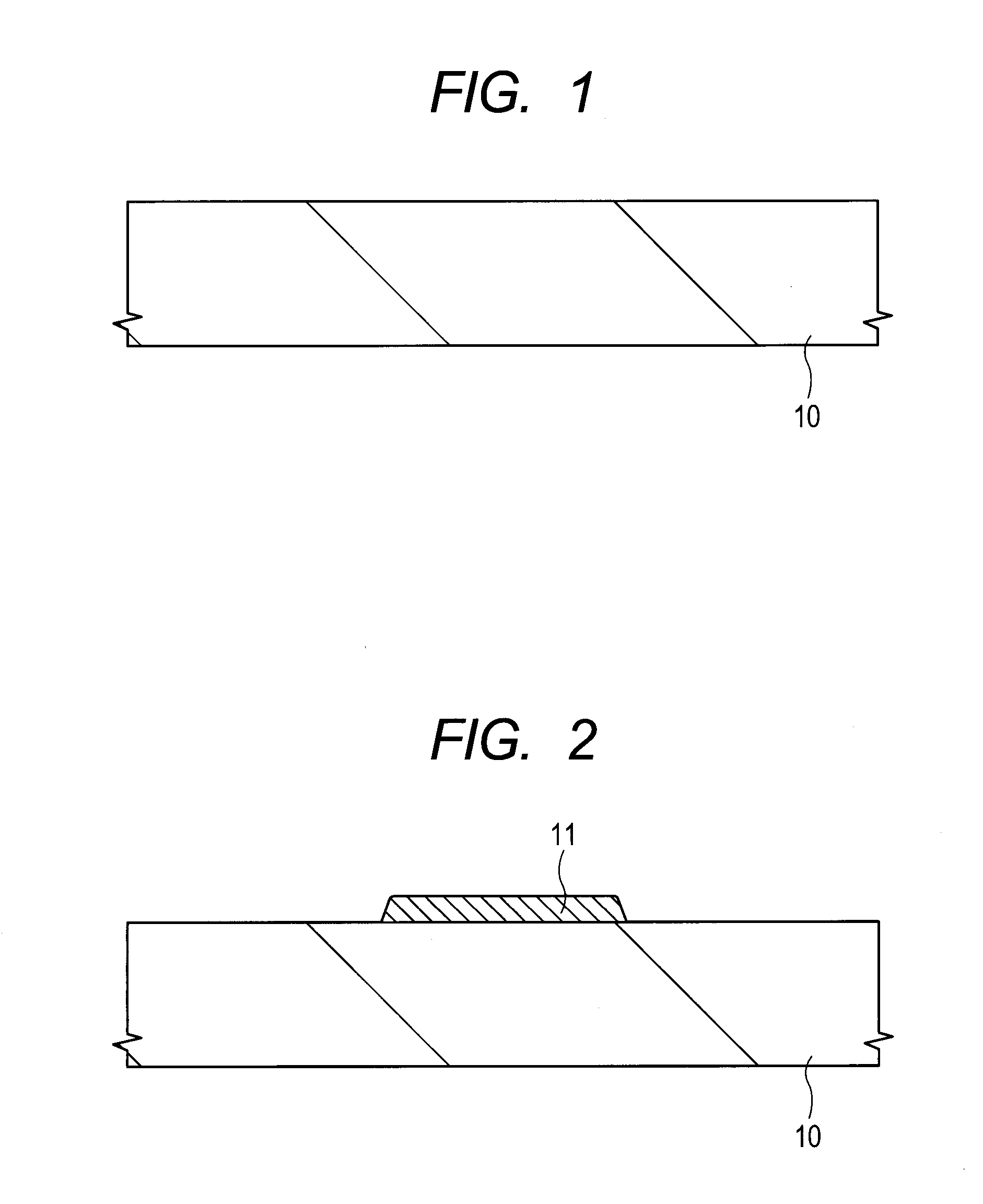
[0047]First, as shown in FIG. 1, an insulating substrate 10 is provided. The material of the substrate 10 is, for example, silicon (Si), sapphire, quartz, glass, or flexible resin sheet (what is called plastic film). The resin sheet material is, for example, polyethylene terephthalate, polyethylene naphthalate, polyetherimide, polyacrylate, polyimide, polycarbonate, cellulose triacetate, or cellulose triacetate propionate. In addition, a substrate with an insulating coating on the surface of the above substrate material may be used a...

second embodiment

[0069]Using the same materials and processes as in the first embodiment, three types of thin-film transistors which have different film thicknesses of the high concentration region (13d), namely (1) 6 nm or less, (2) 20nm, and (3) 50 nm, were produced to study the relation between high concentration region film thickness and sub-threshold slope. Here, the difference between the maximum In concentration of the high concentration region and the In concentration of the other regions was 40 at % or more. FIG. 9 shows the result of the study. Also, for comparison, the relation between the film thickness of an oxide semiconductor layer of In—Ga—Zn—O (IGZO) and the sub-threshold slope is shown in FIG. 9.

[0070]As shown in FIG. 9, when the film thickness of the high concentration region is 6 nm or less, the sub-threshold slope is about 70 mV / decade, and when the film thickness is 20 nm, the sub-threshold slope is 100 mV / decade max. As the film thickness of the high concentration region incre...

third embodiment

[0073]For comparison in effect between the presence and absence of the high concentration region (13D), a thin-film transistor (sample A) having a high concentration region in the oxide semiconductor layer (13) and a thin-film transistor (sample B) having no high concentration region in the oxide semiconductor layer (13) were produced. The oxide semiconductor layer of sample A was made of In—Sn—Zn—O and the oxide semiconductor layer of sample B was made of In—Ga—Zn—O. The materials and processes used for the components other than the oxide semiconductor layer were the same as in the first embodiment.

[0074]FIG. 10 shows the result of analysis by a secondary ion mass spectrometer (SIMS) of composition distribution of constituent elements from the oxide semiconductor layer surface of sample A to the surface of the gate insulating film (12). From this figure, it is known that the oxide semiconductor layer of sample A has a high concentration region with a film thickness of about 6 nm an...


PUM


Abstract

Disclosed is an oxide semiconductor layer (13) which forms a channel for a thin-film transistor and which includes at least In and oxygen and one or more types of elements from among Zn, Cd, Al, Ga, Si, Sn, Ce, and Ge. A high concentration region (13d) is disposed on one section of the oxide semiconductor layer (13), whereby said region has a maximum In concentration 30 at %; or higher than other regions on the oxide semiconductor layer (13). The film thickness of the oxide semiconductor layer (13) is 100 nm max., and the film thickness of the high concentration region (13d) is 20 nm max. or, preferably, 6 nm max. This enables a thin-film transistor with a sub-threshold slope of 100 mV / decade max., a high on-current, and a high field effect mobility to be achieved.

Description

TECHNICAL FIELD[0001]The present invention relates to a semiconductor device, an RFID tag using the same, and an electronic device such as a display device and more particularly to a technique useful for a semiconductor device having a thin-film transistor (TFT) which uses oxide semiconductor for a channel layer.BACKGROUND ART[0002]A thin-film transistor (TFT) is used as a transistor for driving the display device of a mobile device such as a mobile phone, notebook-sized personal computer, tablet computer or PDA because its element area is small and it is space-saving.[0003]In the past, most of thin-film transistors have been made of a silicon-based semiconductor material, typically amorphous silicon or polycrystalline silicon. However, a thin-film transistor which uses a silicon-based semiconductor material has a problem that its sub-threshold slope is as large as about 200 mV / decade and if this thin-film transistor is used to form a circuit, operation at a low voltage of about 1 t...

Claims


Application Information

Patent Timeline
Patent Type & Authority Applications(United States)
IPC IPC(8): H01L29/786
CPCH01L29/7869
Inventor WAKANA, HIRONORIKAWAMURA, TETSUFUMIUCHIYAMA, HIROYUKIFUJII, KUNIHARU
Owner HITACHI LTD
Why Eureka
Try Eureka