

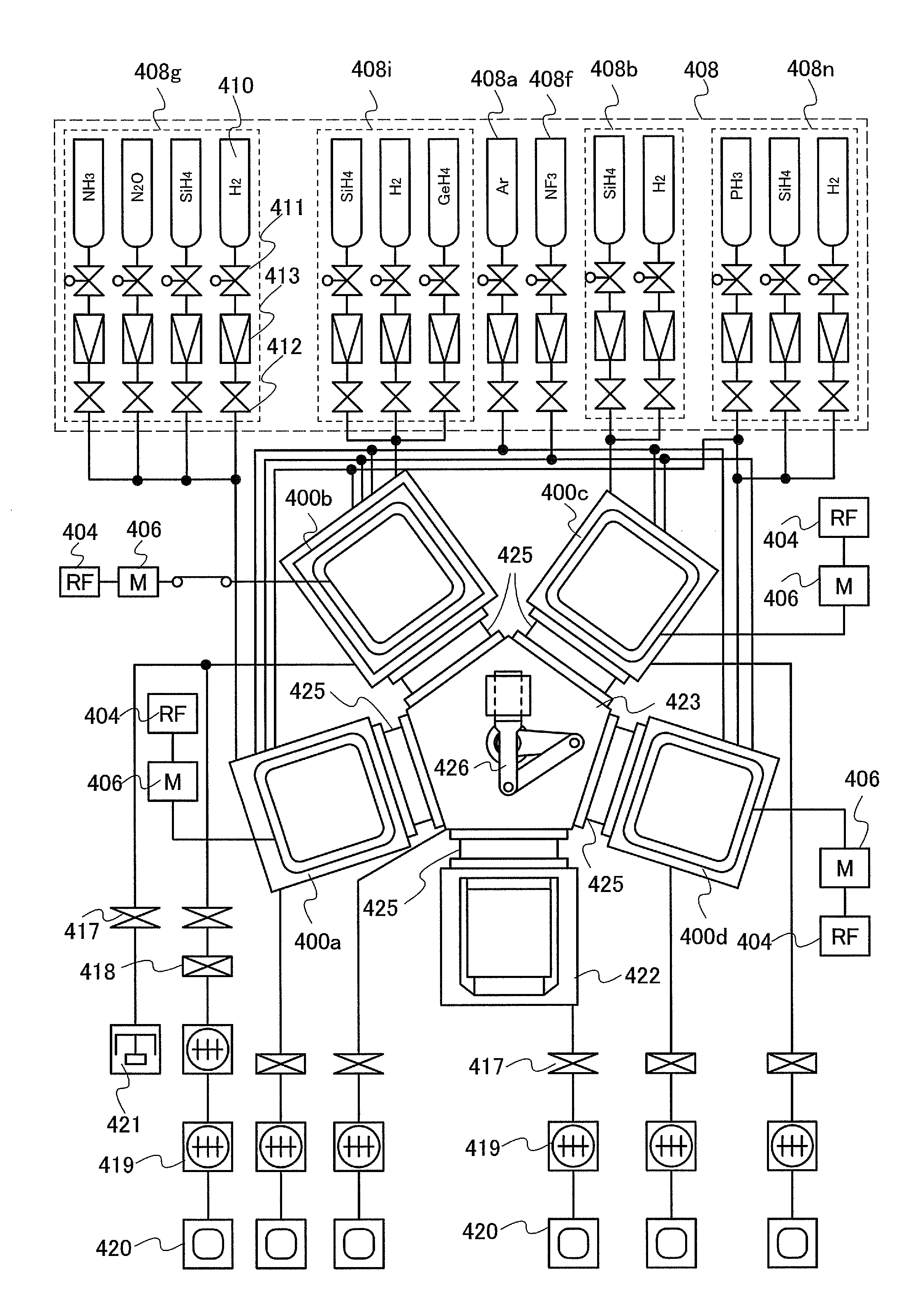
Semiconductor device
a thin film transistor and semiconductor technology, applied in the direction of semiconductor devices, transistors, electrical equipment, etc., can solve the problems of increasing cost, reducing yield, and film requires a more complicated process, so as to reduce the off-current of thin film transistors, reduce the resistance, and improve the mobility of on-current and field effects
- Summary
- Abstract
- Description
- Claims
- Application Information
AI Technical Summary
Benefits of technology
Problems solved by technology
Method used
Image

Examples
embodiment mode 1
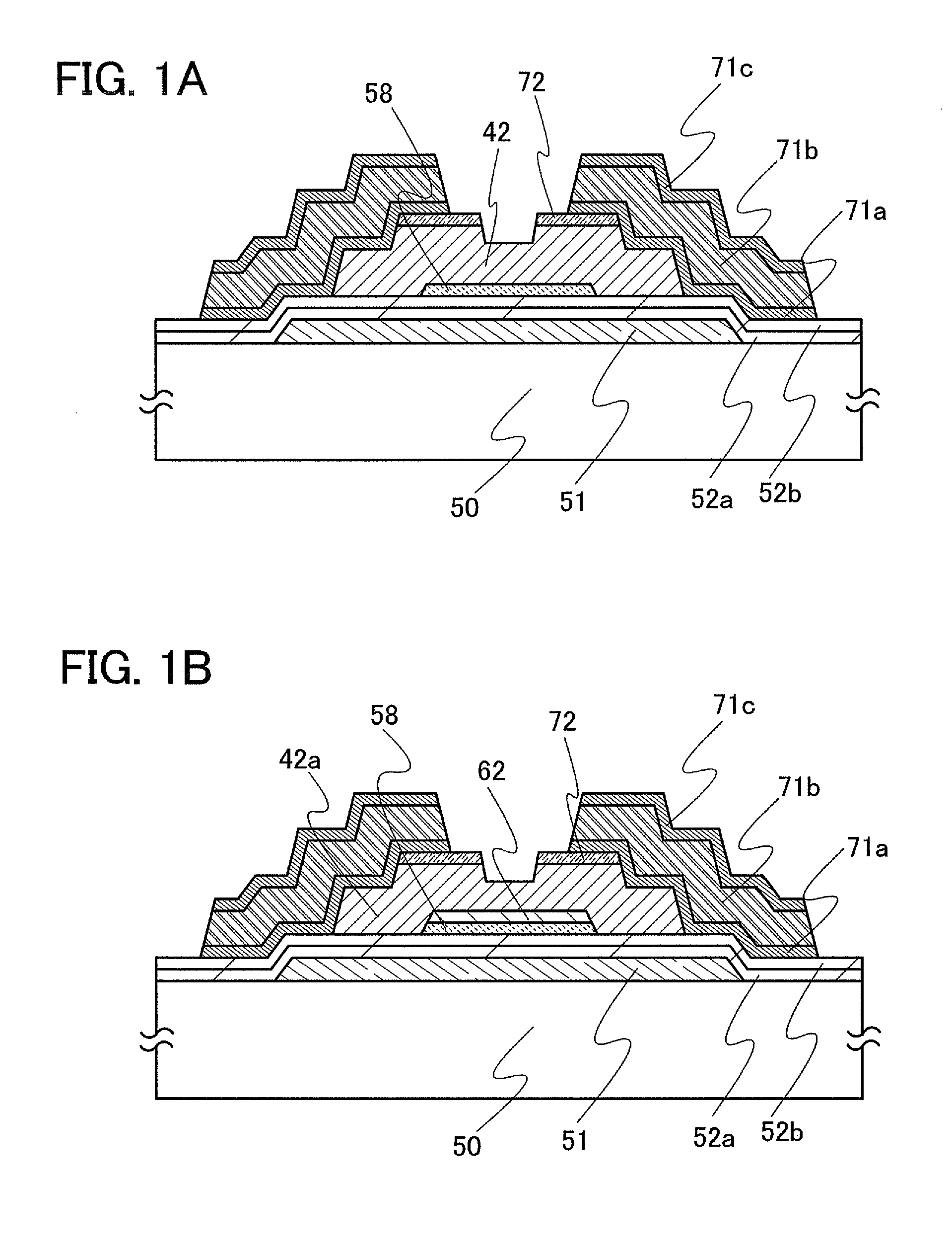
[0070]Here, a structure of a thin film transistor having a higher field effect mobility and on-current and lower off-current than a conventional thin film transistor using a microcrystalline semiconductor film for a channel formation region is described with reference to FIGS. 1A and 1B, FIG. 2, FIG. 3, FIG. 4, FIG. 5, FIG. 6, FIG. 7, FIGS. 8A to 8C, FIGS. 9A to 9F, and FIGS. 10A to 10C.
[0071]In a thin film transistor illustrated in FIG. 1A, a gate electrode 51 is formed over a substrate 50, gate insulating films 52a and 52b are formed over the gate electrode, a semiconductor film 58 to which an impurity element serving as a donor is added is formed over the gate insulating film 52b, a buffer layer 42 is formed over the semiconductor film 58 to which an impurity element serving as a donor is added, a pair of source and drain regions 72 to which an impurity element serving as a donor is added is formed over the buffer layer 42, and wirings 71a to 71c are formed over the pair of sourc...
embodiment mode 2
[0123]In this embodiment mode, another structure of the thin film transistor of Embodiment Mode 1 is described with reference to FIG. 1A and FIGS. 40A and 40B. Although FIG. 1A is referred to here, this embodiment mode can be applied as appropriate to the thin film transistors of other drawings described in Embodiment Mode 1.
[0124]In FIG. 1A, the end portions of the pair of source and drain regions 72 serving as source and drain regions and the semiconductor film 58 to which an impurity element serving as a donor is added overlap.
[0125]In addition, in the thin film transistor illustrated in FIG. 40A, the end portions of the pair of source and drain regions 72 serving as source and drain regions and the end portions of the semiconductor film 58 to which an impurity element serving as a donor is added overlap. In a thin film transistor in which the end portions of the pair of source and drain regions 72 serving as source and drain regions and the end portions of the semiconductor film...
embodiment mode 3
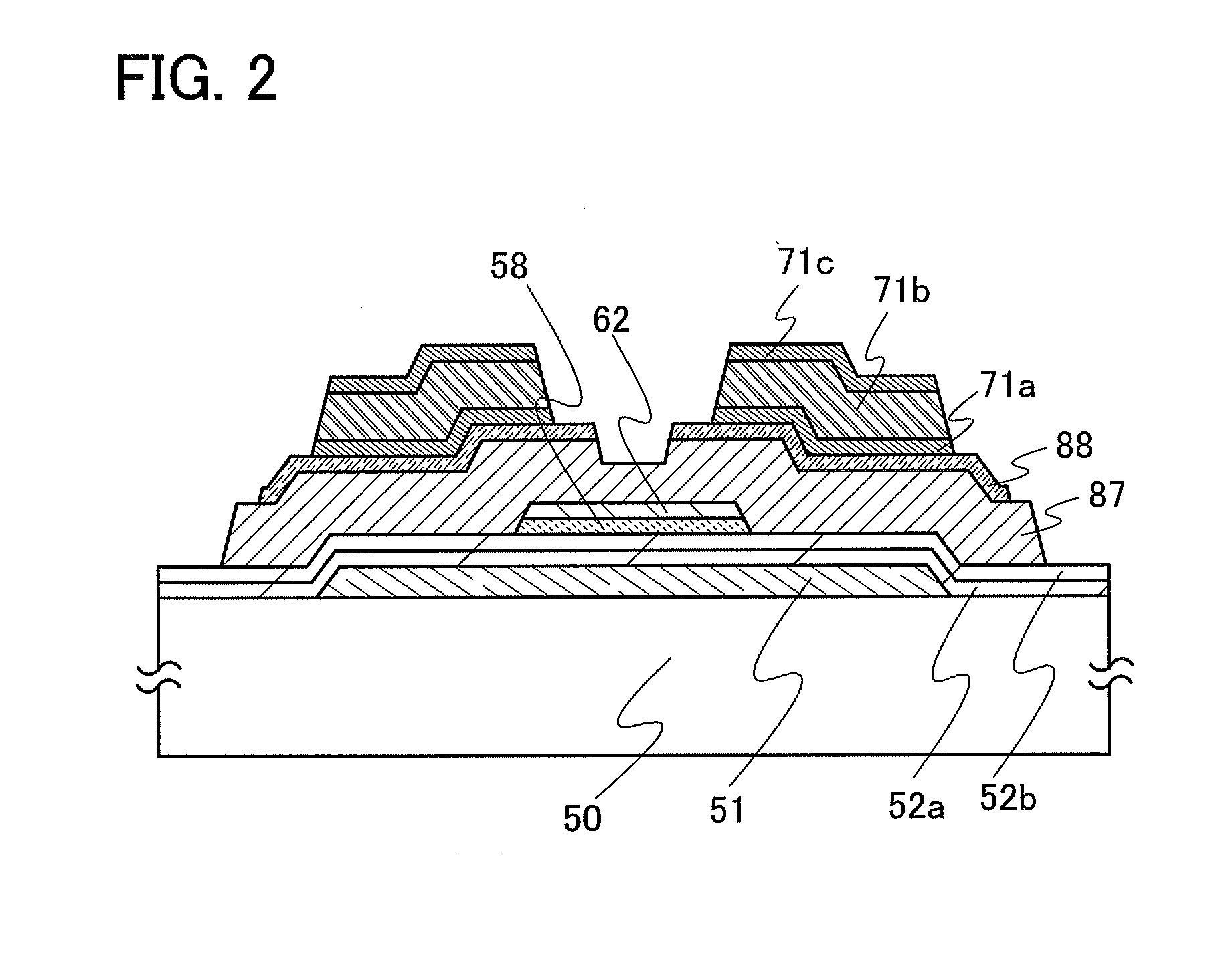
[0127]In this embodiment mode, a manufacturing process for a thin film transistor having high field effect mobility and on-current, and low off-current is described. Here, as a typical example, method for manufacturing the thin film transistor of FIG. 1B in Embodiment Mode 1 is described.
[0128]An n-type thin film transistor having an amorphous semiconductor film or a microcrystalline semiconductor film has higher field effect mobility than a p-type thin film transistor having an amorphous semiconductor film or a microcrystalline semiconductor film, and therefore is more suitable for being used in a driver circuit. It is desired that all thin film transistors formed over one substrate have the same polarity in order to reduce the number of manufacturing steps. Here, description is made using an n-channel thin film transistor.
[0129]As illustrated in FIG. 10A, the gate electrode 51 is formed over the substrate 50, and the gate insulating films 52a and 52b are formed over the gate elect...
PUM
 Abstract
Description
Claims
Application Information