Tunnel Field-Effect Transistor with Metal Source

Inactive Publication Date: 2010-05-20
TAIWAN SEMICON MFG CO LTD
View PDF29 Cites 35 Cited by
  • Summary
  • Abstract
  • Description
  • Claims
  • Application Information

AI Technical Summary

Benefits of technology

[0011]The advantageous features of the present invention include

Problems solved by technology

This limitation is due to the drift-diffusion transport mechanism of carriers.
For this reason, existing MOS devices typically cannot switch faster than 60 mV/decade at room temperatures.
However, even with better gate control over the channel, an ultra-thin body MOSFET on SOI or FinFET can only achieve close to, but not below, the limit of 60 mV/decade.
With such a limit, faster s

Method used


Image

  • Tunnel Field-Effect Transistor with Metal Source
  • Tunnel Field-Effect Transistor with Metal Source
  • Tunnel Field-Effect Transistor with Metal Source

Examples


Embodiment Construction

[0018]The making and using of the presently preferred embodiments are discussed in detail below. It should be appreciated, however, that the present invention provides many applicable inventive concepts that can be embodied in a wide variety of specific contexts. The specific embodiments discussed are merely illustrative of specific ways to make and use the invention, and do not limit the scope of the invention.

[0019]Novel tunnel field-effect transistors (FETs) having metal sources and the methods of forming the same are provided. The intermediate stages of manufacturing preferred embodiments of the present invention are illustrated. The variations of the preferred embodiments are then discussed. Throughout the various views and illustrative embodiments of the present invention, like reference numbers are used to designate like elements.

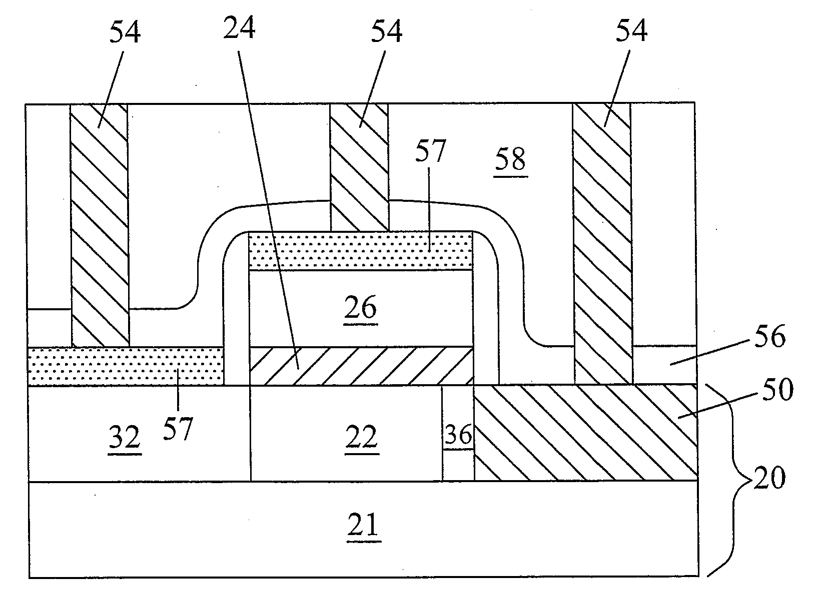
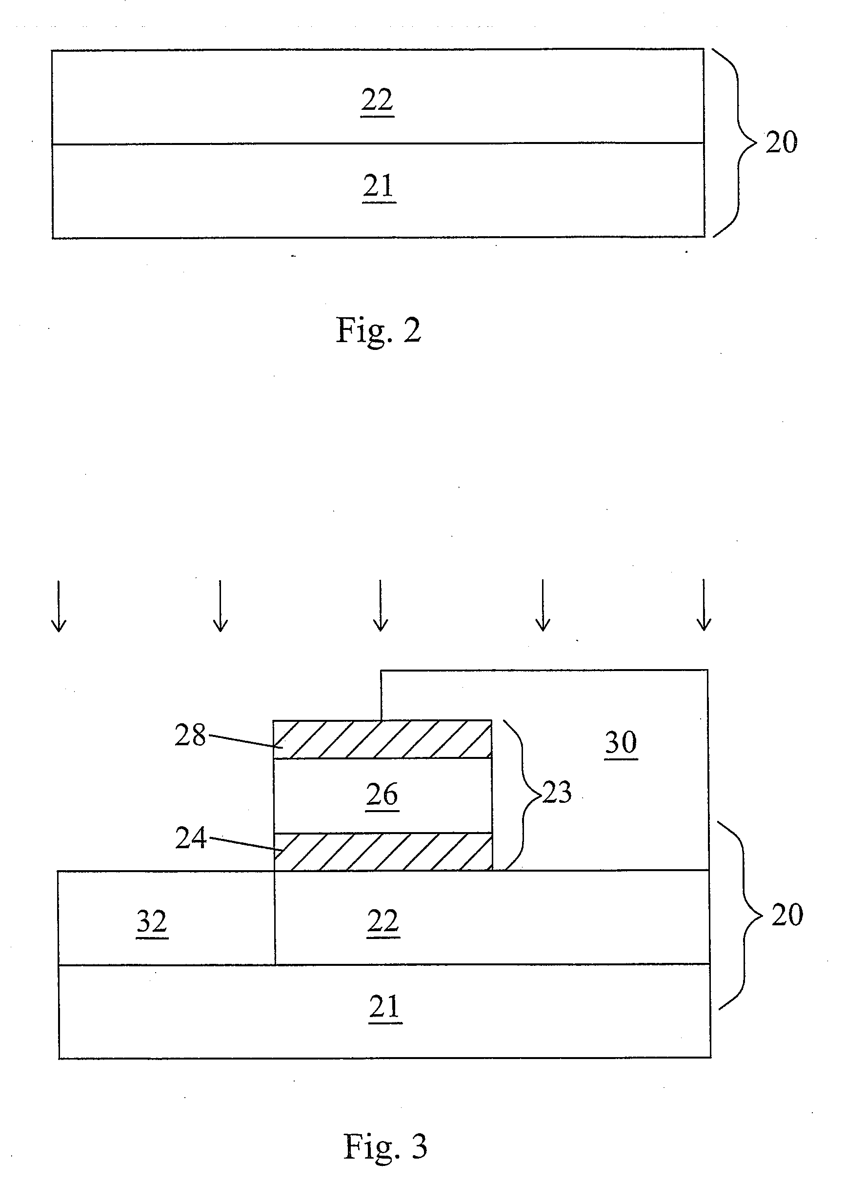
[0020]The formation of an embodiment of the present invention is provided in FIGS. 2 through 7. Referring to FIG. 2, substrate 20 is provided. In an...


PUM


Abstract

A semiconductor device includes a channel region; a gate dielectric over the channel region; and a gate electrode over the gate dielectric. A first source/drain region is adjacent the gate dielectric, wherein the first source/drain region is a semiconductor region and of a first conductivity type. A second source/drain region is on an opposite side of the channel region than the first source/drain region, wherein the second source/drain region is a metal region. A pocket region of a second conductivity type opposite the first conductivity type is horizontally between the channel region and the second source/drain region.

Description

CROSS-REFERENCE TO RELATED APPLICATIONS[0001]This application relates to the following commonly assigned U.S. patent applications: application Ser. No. 11 / 828,211, filed Jul. 25, 2007, and entitled “Tunnel Field-Effect Transistor with Narrow Band-Gap Channel and Strong Gate Coupling;” and application Ser. No. 12 / 205,585, filed Sep. 5, 2008, and entitled “Tunnel Field-Effect Transistors with Superlattice Channels,” which applications are hereby incorporated herein by reference.TECHNICAL FIELD[0002]This invention relates generally to semiconductor devices, and more specifically to tunnel field-effect transistors (FETs) having metal sources.BACKGROUND[0003]Metal-oxide-semiconductor (MOS) is a dominating technology for integrated circuits at 90 nm technology and beyond. A MOS device can work in three regions, depending on gate voltage Vg and source-drain voltage Vds, linear, saturation, and sub-threshold regions. The sub-threshold region is a region wherein gate voltage Vg is smaller th...

Claims


Application Information

Patent Timeline
IPC IPC(8): H01L29/78
CPCH01L29/7391H01L29/66356
Inventor BHUWALKA, KRISHNA KUMARSHEU, YI-MINGDIAZ, CARLOS H.
Owner TAIWAN SEMICON MFG CO LTD
Why Eureka
Try Eureka