Semiconductor thin film, thin film transistor, method for manufacturing same, and manufacturing equipment of semiconductor thin film

a technology of semiconductor thin film and manufacturing method, which is applied in the direction of semiconductor devices, transistors, electrical devices, etc., can solve the problems of high processing time, low-softening point glass having a low softening point cannot be used, and poly-crystalline silicon tft has a disadvantage, etc., to achieve the maintenance life of the energy beam irradiation device, the effect of large size and short formation tim

Active Publication Date: 2006-05-23
VISTA PEAK VENTURES LLC
View PDF8 Cites 33 Cited by
  • Summary
  • Abstract
  • Description
  • Claims
  • Application Information

AI Technical Summary

Benefits of technology

[0053]Thus, according to the present invention, since such the projection exposure unit as above is provided, the semiconductor thin film whose crystal grains having a uniform direction of crystal growth and being large in size can be formed effectively in a very short time.
[0054]With the above configurations, unlike in the conventional case in which several tens times to several hundreds times beam irradiation is required to re-crystallize a semiconductor thin film on a substrate having even a big area size of, for example, 1 m square, by one pulse irradiation, re-crystallization of the semiconductor thin film on an entire surface of a substrate can be realized. As a result, a process of irradiating a laser beam is speeded up several tens times to several hundreds times and a maintenance life of the energy beam irradiation device can be made very long.
[0055]With another configurations, since a big crystal can be grown in a specified direction, by matching a running direction of a carrier with a direction of growth of a crystal, unlike in the conventional method in which a channel is formed in a semiconductor thin film having polycrystalline grains arranged randomly, a high on-current with a high mobility can be obtained. As a result, an integrated circuit whose driving voltage is lower than that of an integrated circuit made up of thin film transistors formed on a glass substrate by the conventional method and whose operating speed is high can be achieved and, when the integrated circuit of the present invention is employed, for example, in a liquid crystal display, both a pixel TFT to drive each pixel and a peripheral driving circuit are simultaneously formed on a same glass substrate, which serves to enable manufacturing process costs to be reduced and peripheral driver integrated circuits to be miniaturized and enables creation of new electronic devices.
[0056]With still another configurations, since the irradiation device having an optical device with high resolution is provided, a local temperature gradient which enables growth of the crystal to occur in a desired direction with a light-shielded region as a starting point can be given to the light-shielded region in which light is intercepted by the light-shielding element. As a result, melt and re-crystallization of a semiconductor thin film can be very effectively performed. A remarkable effect, in particular, is that melt and re-crystallization can be achieved by one pulse irradiation even if a semiconductor thin film has a large area.

Problems solved by technology

However, the poly-crystalline silicon TFT has a disadvantage.
That is, since the high-temperature process of about 100° C. is performed when the poly-crystalline silicon is manufactured, a low-priced glass having a low-softening point cannot be used, unlike in the case of the hydrogenated amorphous silicon TFT.
However, since its movement distance is as short as about 1 μm, it takes much time to complete the processing in a specified region.

Method used


Image

  • Semiconductor thin film, thin film transistor, method for manufacturing same, and manufacturing equipment of semiconductor thin film
  • Semiconductor thin film, thin film transistor, method for manufacturing same, and manufacturing equipment of semiconductor thin film
  • Semiconductor thin film, thin film transistor, method for manufacturing same, and manufacturing equipment of semiconductor thin film

Examples


first embodiment

A Method for Manufacturing Semiconductor Thin Film

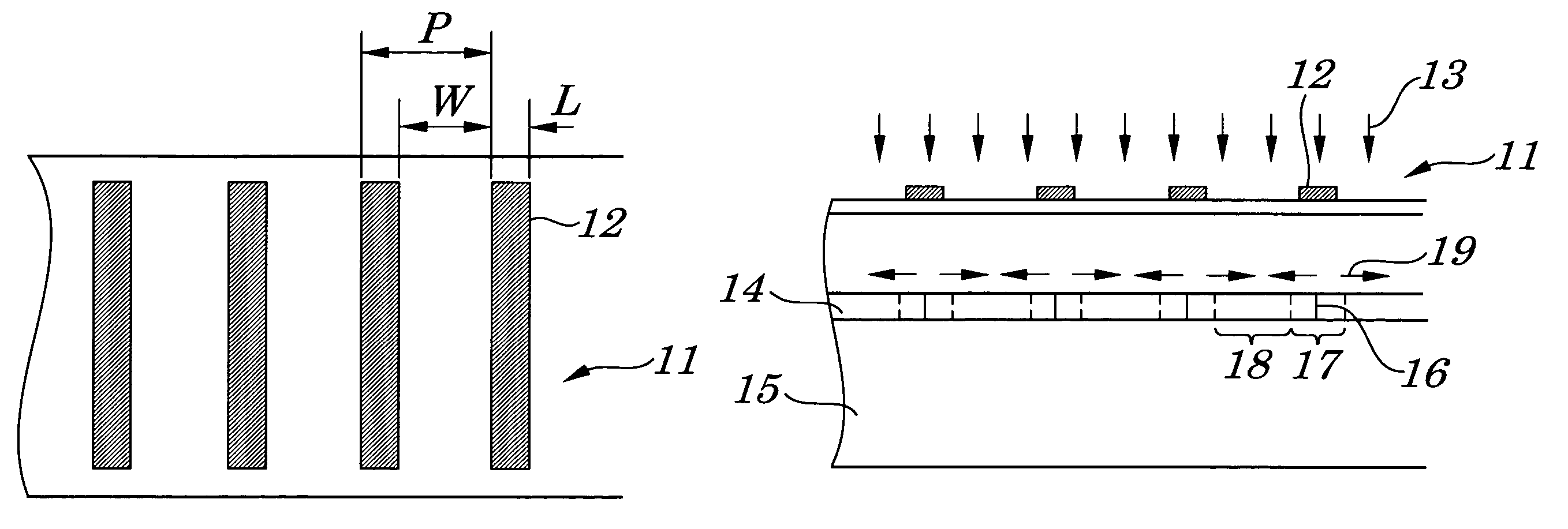
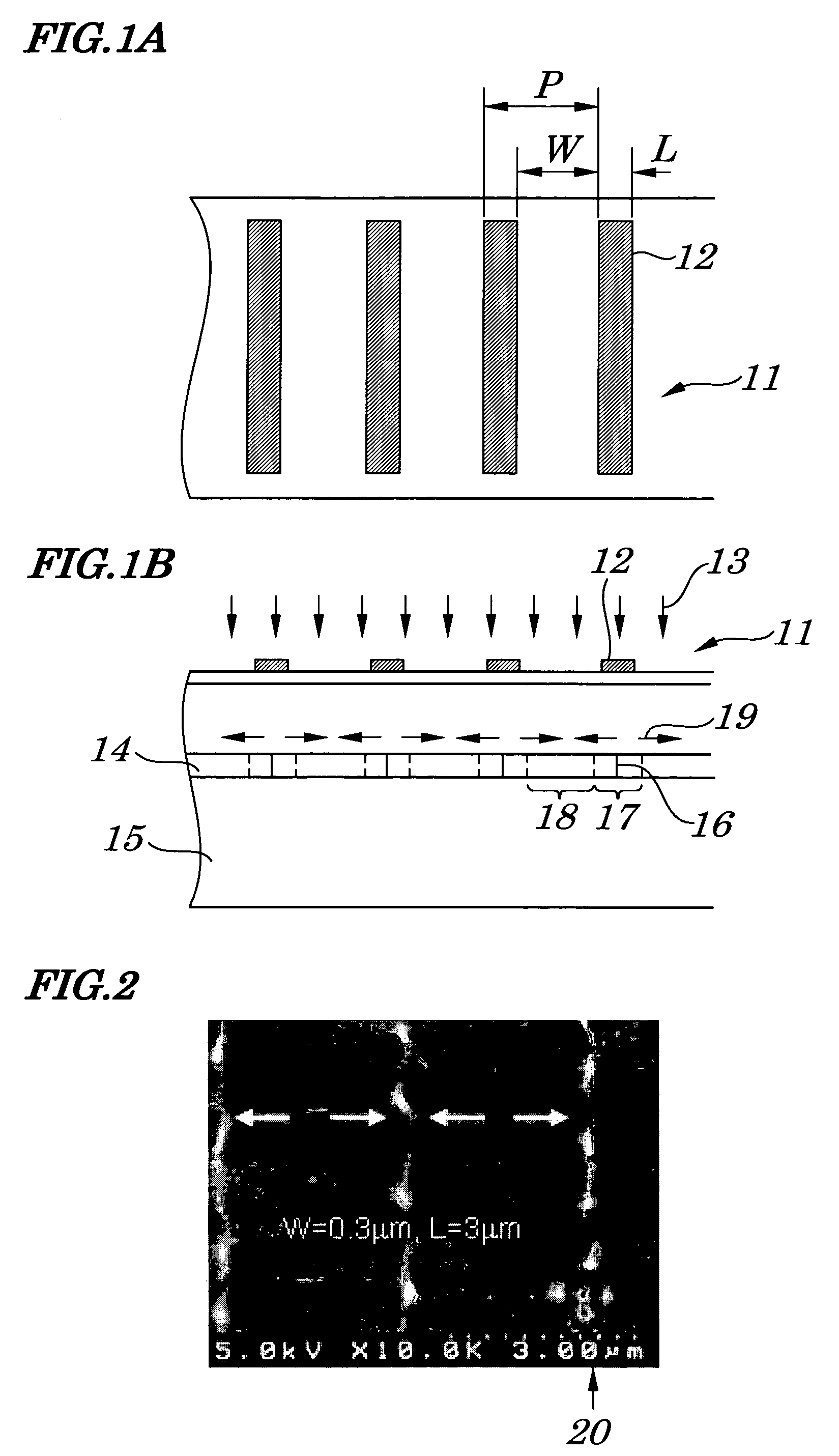
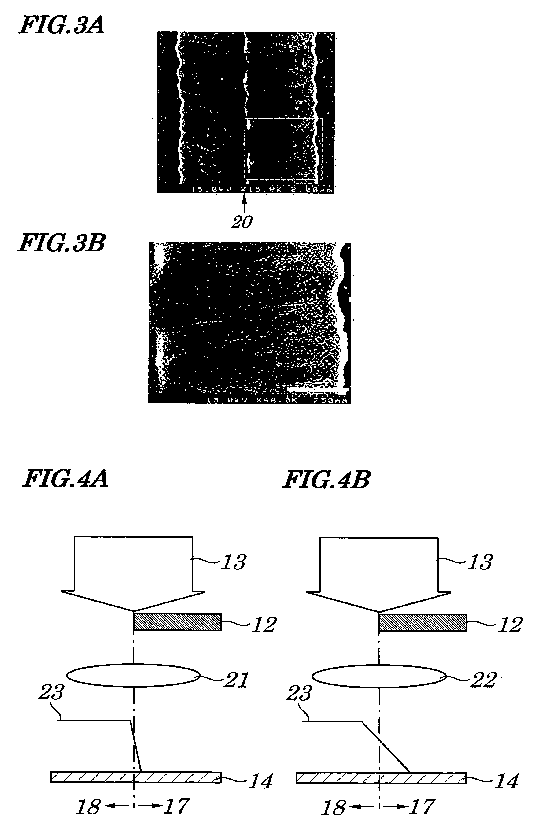
[0078]FIGS. 1A and 1B are diagrams explaining a method for manufacturing a semiconductor thin film according to a first embodiment of the present invention. FIG. 1A is a plan view illustrating one example of light-shielding elements employed in the present invention. FIG. 1B is a schematic cross-sectional view explaining melt and re-crystallization occurring in a semiconductor thin film irradiated with a beam employed in the present invention. FIG. 2 shows a photograph of a magnified plan view of a growth state of a silicon crystal observed when melt and re-crystallization have been performed by using the light-shielding mask as shown in FIG. 1A. FIGS. 3A and 3B show photographs of a magnified plan view of a state of a crystal growing in the same direction as a temperature gradient direction (in a horizontal direction).

[0079]The light-shielding elements are placed between a beam source and an object to be irradiated (in an upper port...

second embodiment

Another Method for Manufacturing Semiconductor Thin Film

[0125]Next, a method for manufacturing semiconductor thin film according to a second embodiment of the present invention will be described. By employing the method for manufacturing a semiconductor thin film of the present invention described above, as shown in FIG. 14, a silicon crystal could be grown radially by melt and re-crystallization.

[0126]For example, the silicon crystal shown in FIG. 14 is obtained by using the light-shielding mask in which dot-shaped light-shielding patterns each having a diameter of 1.5 μm are placed at an equal interval pitch of about 4 μm and applying an excimer laser with a wavelength of 308 nm and with an energy intensity of 467 mJ / cm2 to a silicon thin layer with a thickness of 60 μm. As is understood from FIG. 14, the silicon crystal grows radially from the light-shielded region and no clearance is observed between the silicon crystal having grown from the light-shielded region and the silicon...

third embodiment

A Method for Manufacturing TFT

[0127]Next, a method for manufacturing TFT according to a third embodiment of the present invention will be described. The method for manufacturing a semiconductor thin film described above is applied to manufacturing of a TFT according to the embodiment. An example of the method for manufacturing a TFT that can obtain a crystallized film in a desired region in a self-aligning manner is explained by referring to a process flow diagram shown in FIGS. 15A to 15I, and FIG. 15I′.

[0128]That is, in the method for manufacturing a TFT of the present invention, a crystallized film whose crystal grows in one direction with a light-shielded region of a semiconductor thin film as a starting point is formed by using a gate electrode formed on the semiconductor thin film with a gate insulating film being interposed between the gate electrode and the semiconductor thin film as a light-shielding element and by applying an energy beam to the semiconductor thin film. Thu...


PUM

PropertyMeasurementUnit
light-shielding widthaaaaaaaaaa
widthaaaaaaaaaa
softening pointaaaaaaaaaa

Abstract

A method for manufacturing a semiconductor thin film is provided which can form its crystal grains having a uniform direction of crystal growth and being large in size and a manufacturing equipment using the above method, and a method for manufacturing a thin film transistor. In the above method, by applying an energy beam partially intercepted by a light-shielding element, melt and re-crystallization occur with a light-shielded region as a starting point. The irradiation of the beam gives energy to the light-shielded region of the silicon thin film so that melt and re-crystallization occur with the light-shielded region as the starting point and so that a local temperature gradient in the light-shielded region is made to be 1200° C./μm or more. In the manufacturing method, a resolution of an optical system used to apply the energy beam is preferably 4 μm or less.

Description

BACKGROUND OF THE INVENTION[0001]1. Field of the Invention[0002]The present invention relates to a method for manufacturing a semiconductor thin film making up a semiconductor device, such as memory and CPU (Central Processing Unit), a thin film transistor (TFT) made up of a same semiconductor thin film, and a method for manufacturing the same semiconductor thin film and the same TFT, and a manufacturing equipment being used in manufacturing the same semiconductor thin film.[0003]The present application claims priority of Japanese Patent Application No. 2003-131405 filed on May 9, 2003, which is hereby incorporated by reference.[0004]2. Description of the Related Art[0005]A conventional product manufactured by forming a semiconductor integrated circuit on a glass substrate is typified by a TFT. A conventional typical TFT is constructed, as shown in FIG. 17, by forming a channel region 103, a source region 104, a drain region 105, and an LDD (Lightly-doped drain) region 106 on a glas...

Claims


Application Information

Patent Timeline
Patent Type & Authority Patents(United States)
IPC IPC(8): H01L21/84H01L21/20H01L21/268H01L21/336H01L29/786
CPCH01L21/2026H01L29/66757H01L29/78633H01L29/786H01L21/268H01L29/04H01L29/78675H01L21/0262H01L21/02686H01L21/02422H01L21/02532
Inventor TANABE, HIROSHI
Owner VISTA PEAK VENTURES LLC
Why Eureka
Try Eureka