Semiconductor device having STI with nitride liner

Active Publication Date: 2006-01-05
FUJITSU SEMICON LTD
View PDF15 Cites 34 Cited by
  • Summary
  • Abstract
  • Description
  • Claims
  • Application Information

AI Technical Summary

Benefits of technology

[0021] It is possible to prevent ultraviolet rays from being irradiated

Problems solved by technology

Namely, the ratio of narrowing the element forming region increases, hindering the high integration of semiconductor devices.
Alt

Method used


Image

  • Semiconductor device having STI with nitride liner
  • Semiconductor device having STI with nitride liner
  • Semiconductor device having STI with nitride liner

Examples


Embodiment Construction

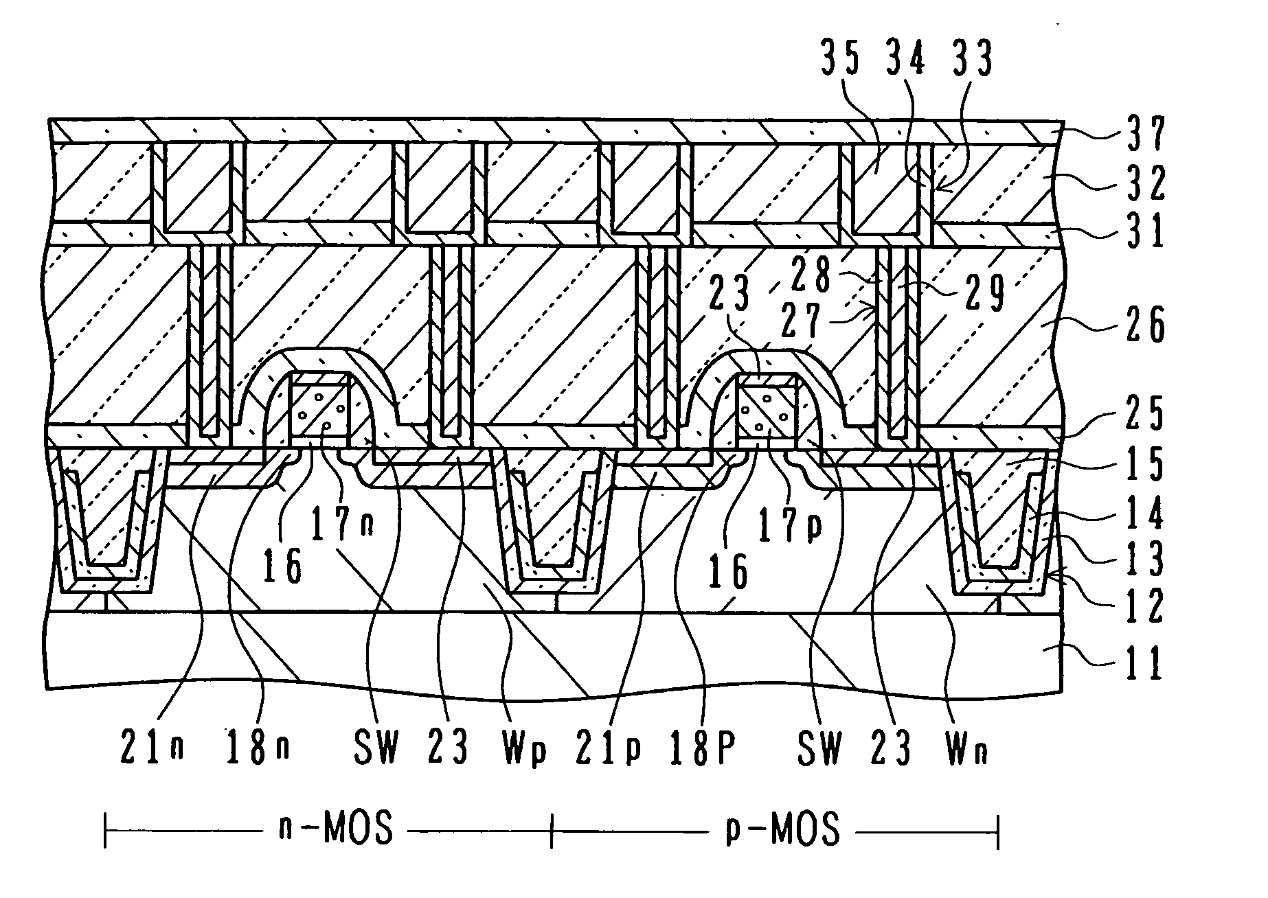
[0028] Prior to the description of the preferred embodiments of the invention, the results of studies made by the present inventor will be described. A silicon nitride layer was formed on a buffer silicon oxide layer formed on the surface of a silicon substrate. A resist pattern was formed on the silicon nitride layer and a shallow trench was formed in the silicon substrate by etching. The silicon surface exposed in the trench was thermally oxidized and a silicon nitride layer liner was formed in the trench. A silicon oxide was deposited by high density plasma (HDP) CVD, burying the trench, and the unnecessary insulating layer on the surface of the silicon substrate was removed by chemical mechanical polishing (CMP) to form a shallow trench isolation (STI). A MOS transistor was formed in an active region defined by STI and multi-layer electrodes were formed. It was found that leak current flowed.

[0029] STI has the liner layer of the silicon oxide layer in contact with the active re...


PUM


Abstract

A semiconductor device has: a silicon substrate; trench formed downward from the surface of the silicon substrate, the trench defining active regions on the surface of the silicon substrate; a first liner layer of a silicon nitride film covering an inner wall of the trench; a second liner layer of a silicon nitride layer formed on the first liner layer; an element isolation region of an insulator formed on the second liner layer; a p-channel MOS transistor formed in and on one of the active regions; a contact etch stopper layer of a silicon nitride layer not having a ultraviolet shielding ability, formed above the silicon substrate, and covering the p-channel MOS transistor; and a light shielding film of a silicon nitride layer having the ultraviolet shielding ability and formed above the contact etch stopper layer.

Description

CROSS REFERENCE TO RELATED APPLICATION [0001] This application is based on and claims priority of Japanese Patent Application No. 2004-192744 filed on Jun. 30, 2004, the entire contents of which are incorporated herein by reference. BACKGROUND OF THE INVENTION [0002] A) Field of the Invention [0003] The present invention relates to a semiconductor device and its manufacture method, and more particularly to a semiconductor device having a shallow trench isolation (STI) and its manufacture method. [0004] B) Description of the Related Art [0005] The local oxidation of silicon, LOCOS, has been used as one of the element isolation methods for semiconductor devices. The local oxidation of silicon is the techniques wherein a silicon oxide layer is formed on a silicon substrate as a buffer layer, thereafter a silicon nitride film is formed as an oxidation preventing mask layer, the silicon nitride layer is patterned and thereafter the surface of the silicon substrate is thermally oxidized. ...

Claims


Application Information

Patent Timeline
IPC IPC(8): H01L29/78H01L21/336
CPCH01L21/3185H01L21/76224H01L21/823878H01L23/53295H01L23/552H01L29/517H01L2924/0002H01L29/518H01L29/665H01L29/7843H01L2924/00H01L21/0217H01L21/02164H01L21/022
Inventor OOKURA, YOSHIYUKI
Owner FUJITSU SEMICON LTD
Why Eureka
Try Eureka