SRAM device

Inactive Publication Date: 2005-05-24
SOCIONEXT INC
View PDF11 Cites 28 Cited by
  • Summary
  • Abstract
  • Description
  • Claims
  • Application Information

AI Technical Summary

Benefits of technology

[0007]A first SRAM device of the present invention is characterized in that the drive transistor and the access transistor of one unit circuit have substantially the same channel width (gate width), and the channel width is larger than that of the drive transistor and the access transistor of the other unit circuit. In this way, it is possible to ensure a large cell current, thereby reducing the bit line amplification delay. Furthermore, if the channel width ratio between the load transistor and the drive transistor of one unit circuit and that of the other unit circuit are set to be different from each other by 15% or more, for example, it is possible to prevent stored data from being lost by potential floating due to a cell current during a read operation.
[0008]A second SRAM device of the present invention is characterized in that the two unit circuits are asymmetric with each other in terms of the magnitude of an off leak current of the inverter. In this way, it is possible to reduce the leak current of the SRAM device on standby, while ensuring a large cell current in one unit circuit.
[0009]A third SRAM device of the present invention is characterized in that the two unit circuits are asymmetric with each other in terms of the thickness of the gate oxide film of the constituent transistors. In this way, it is possible to reduce the gate leak current of the SRAM device on standby, while ensuring a large cell current in one unit circuit.
[0010]A fourth SRAM device of the present invention is characterized in that: a bit line connected to one of the two unit circuits is used only for write operations, whereas a bit line connected to the other unit circuit is used for both read and write operations; the current driving power of at least one of the constituent transistors of one of the unit circuits that is connected to the write-only bit line is set to be lower than that of corresponding one of the constituent transistors of the other unit circuit; and the access transistors of the two unit circuits are configured so that only one of the access transistors is activated during a read operation, whereas both of the access transistors are activated during a write operation. In this way, it is possible to realize a single-ended read, differential write operation.
[0011]A fifth SRAM device of the present invention is characterized in that: the two unit circuits are asymmetric with each other in terms of the current driving power of the constituent transistors; and the SRAM device further includes means for setting, during a read operation, the potential level of the source line of one of the two unit circuits of the lower current driving power to be higher than that of the source line of the other unit circuit. In this way, it is possible to prevent stored data from being lost by potential floating due to a cell current during a read operation, while ensuring a large cell current in one unit circuit.
[0012]A sixth SRAM device of the present invention is characterized in that in each of the two unit circuits, the drive transistor and the access transistor have substantially the same channel width and are formed in the same continuous rectangular-shaped active region with no bent portions. In this way, the stress in the active region is reduced, thereby preventing a defect from occurring.

Problems solved by technology

A smaller cell current means a greater bit line amplification delay.
However, in the first conventional example, the two unit circuits are symmetric in terms of the size of the constituent transistors, whereby in order to increase the cell current to reduce the bit line amplification delay so as to realize a faster operation, it is necessary to increase the size of all of the six transistors, which leads to a substantial increase in the cell area.
In the second conventional technique, the NMOS access transistors of the two units have the same gate width, whereby the current driving power of the NMOS drive transistor having a large gate width cannot be fully made use of.

Method used


Image

  • SRAM device
  • SRAM device
  • SRAM device

Examples


Embodiment Construction

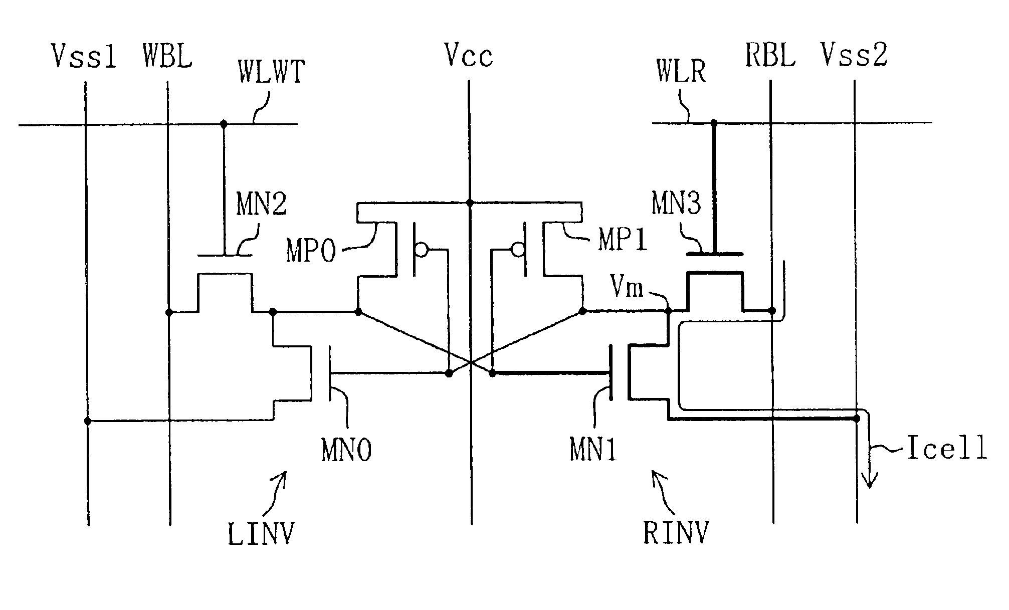
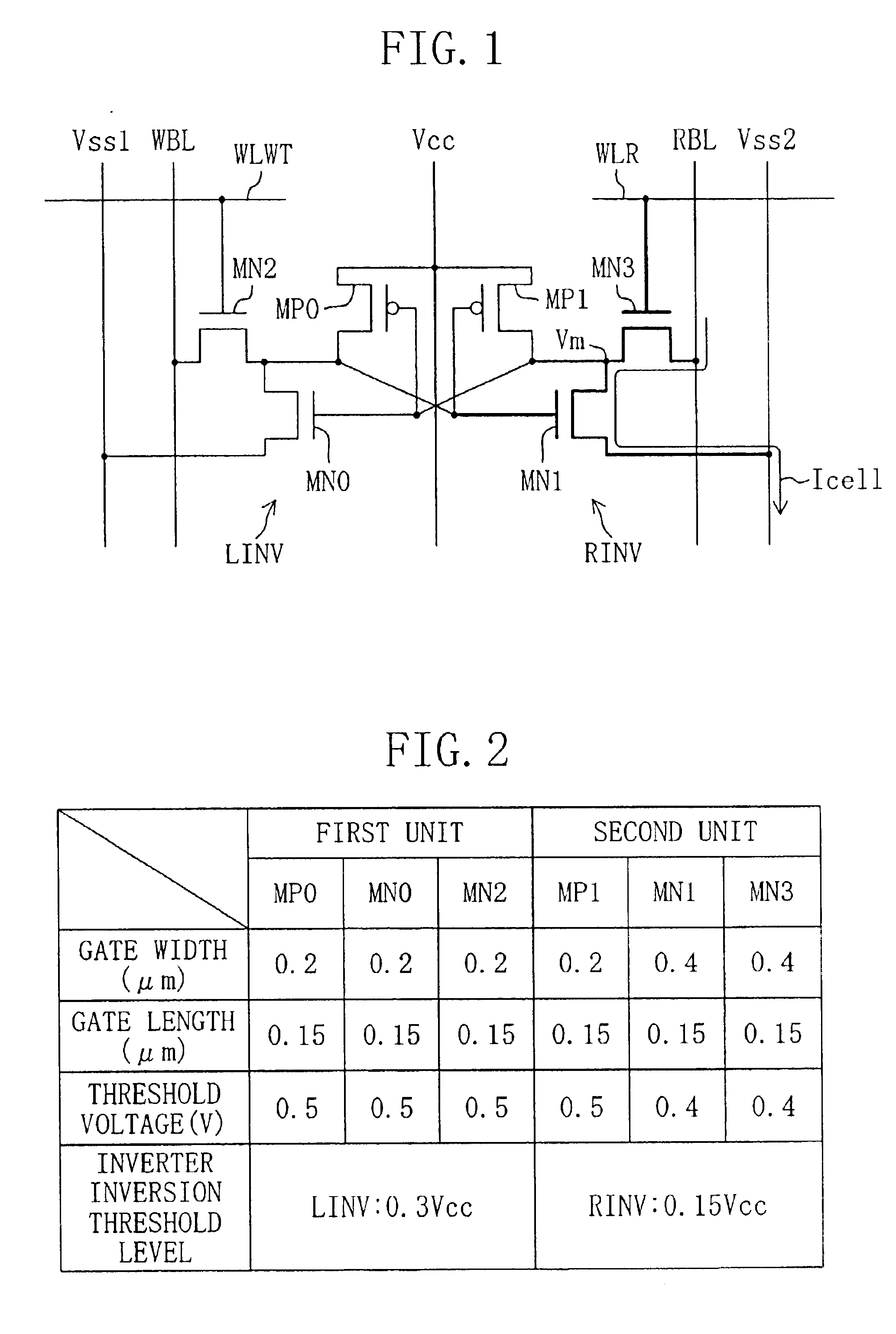
[0022]FIG. 1 illustrates an exemplary configuration of an SRAM device of the present invention. Referring to FIG. 1, the SRAM device includes PMOS load transistors MP0 and MP1, NMOS drive transistors MN0 and MN1, and NMOS access transistors MN2 and MN3. MP0, MN0 and MN2 together form a first unit circuit. MP0 and MN0 together form an inverter (left inverter LINV), and the output of the inverter is connected to a write-only bit line (write bit line) WBL by MN2. The gate of MN2 is connected to a write-only word line (write word line) WLWT, and the source of MN0 is connected to a first source line Vss1. MP1, MN1 and MN3 together form a second unit circuit. MP1 and MN1 together form an inverter (right inverter RINV), and the output of the inverter (i.e., an intermediate node Vm) is connected to a read / write bit line (read bit line) RBL by MN3. The gate of MN3 is connected to a read / write word line (read word line) WLR, and the source of MN1 is connected to a second source line Vss2. The...


PUM


Abstract

In a CMOS type SRAM device having a 6-transistor configuration, only a drive transistor and an access transistor of one unit circuit are designed with a larger size, with the other four transistors having a smaller size.

Description

BACKGROUND OF THE INVENTION[0001]The present invention relates to an SRAM (static random access memory) device in which memory cells can be arranged with a high density.[0002]A CMOS type SRAM device having a 6-transistor configuration is known in the art. Such an SRAM device includes two unit circuits, each including a PMOS load transistor, an NMOS drive transistor and an NMOS access transistor. The PMOS load transistor and the NMOS drive transistor together form an inverter, and the NMOS access transistor connects the output of the inverter to a bit line. The two unit circuits are coupled together by connecting the input and the output of one inverter with those of the other inverter in a cross-coupled manner.[0003]An SRAM device described in U.S. Pat. No. 5,744,844 (first conventional example) employs a lateral-type cell structure in which the PMOS load transistor of each unit is provided in an N-well region that is located in a central area of a memory cell region, the NMOS drive...

Claims


Application Information

Patent Timeline
IPC IPC(8): G11C11/40G11C11/00G11C11/407H01L21/70H01L21/8244H01L27/11G11C7/00
CPCH01L27/1104H10B10/12H10B10/00
Inventor YAMAUCHI, HIROYUKI
Owner SOCIONEXT INC
Why Eureka
Try Eureka