Field-effect transistor

a field-effect transistor and transistor technology, applied in the field of field-effect transistors, can solve the problems of increasing gate leakage current, buried gate structure etc., and achieve the effects of suppressing gate leakage current, reducing the maximum drain current, and small leakage path

Inactive Publication Date: 2007-11-22
MITSUBISHI ELECTRIC CORP
View PDF5 Cites 10 Cited by
  • Summary
  • Abstract
  • Description
  • Claims
  • Application Information

AI Technical Summary

Benefits of technology

[0015]The field-effect transistor according to the present invention produces the following effects. That is, only a lower side wall of the gate electrode buried in the gate buried layer is in contact with the gate buried layer, which suppresses a gate leakage current. Further, a surface level of the gate buried layer affects the maximum drain current only by a recess width, that is, by a distance between an upper side wall of the gate electrode and an inner side wall of a recess provided in the gate buried layer. This can suppress a reduction in the maximum drain current to be small.
[0016]In addition, the gate buried layer and the gate contact layer are undoped and have a doped concentration of equal to or less than 1×1016 cm−3, which can make a leakage path small and suppress the gate leakage current.

Problems solved by technology

However, a use of AlGaAs or AlGaN as the gate contact layer has a problem of reducing the maximum drain current due to an expansion of a surface depletion layer.
A surface of the compound semiconductor generally serves as an interface with a protective insulating film, although the surface has high defect levels, which causes a Fermi level pinning or a transient response of a charge capture / release through the level.
However, when the transistor is normally operated, that is, when the voltage applied between the gate and the drain is 10 V or 20 V, the buried gate structure has a problem in that the gate leakage current is increased.
As described above, there is a problem in that a large gate leakage current causes a large gate current to flow in a case of a high frequency operation, which results in a reduction in gate voltage.
Therefore, it is difficult for the conventionally proposed buried gate structure to increase the maximum drain current and attain the high breakdown voltage at the same time.

Method used


Image

  • Field-effect transistor
  • Field-effect transistor
  • Field-effect transistor

Examples


first embodiment

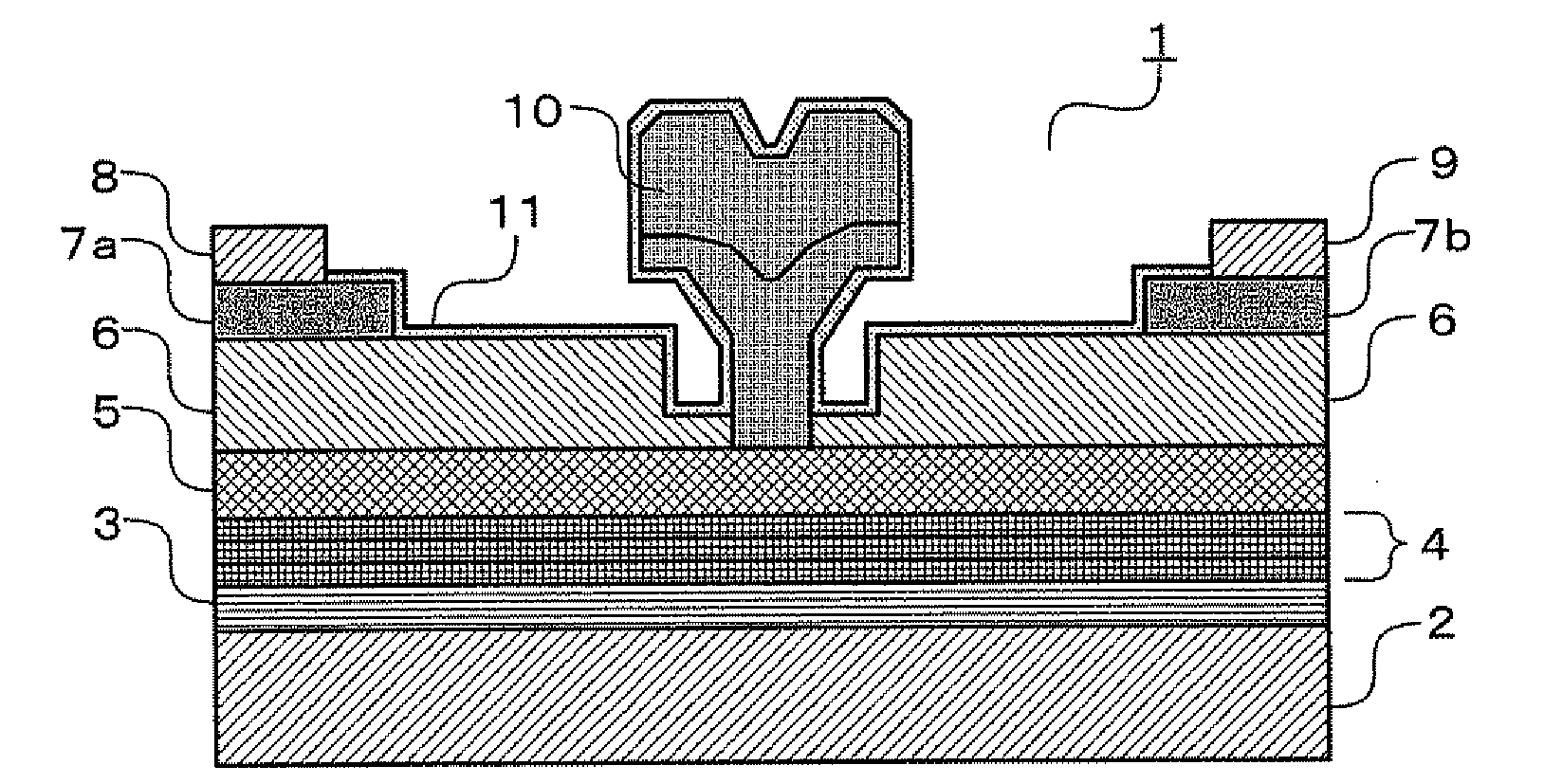
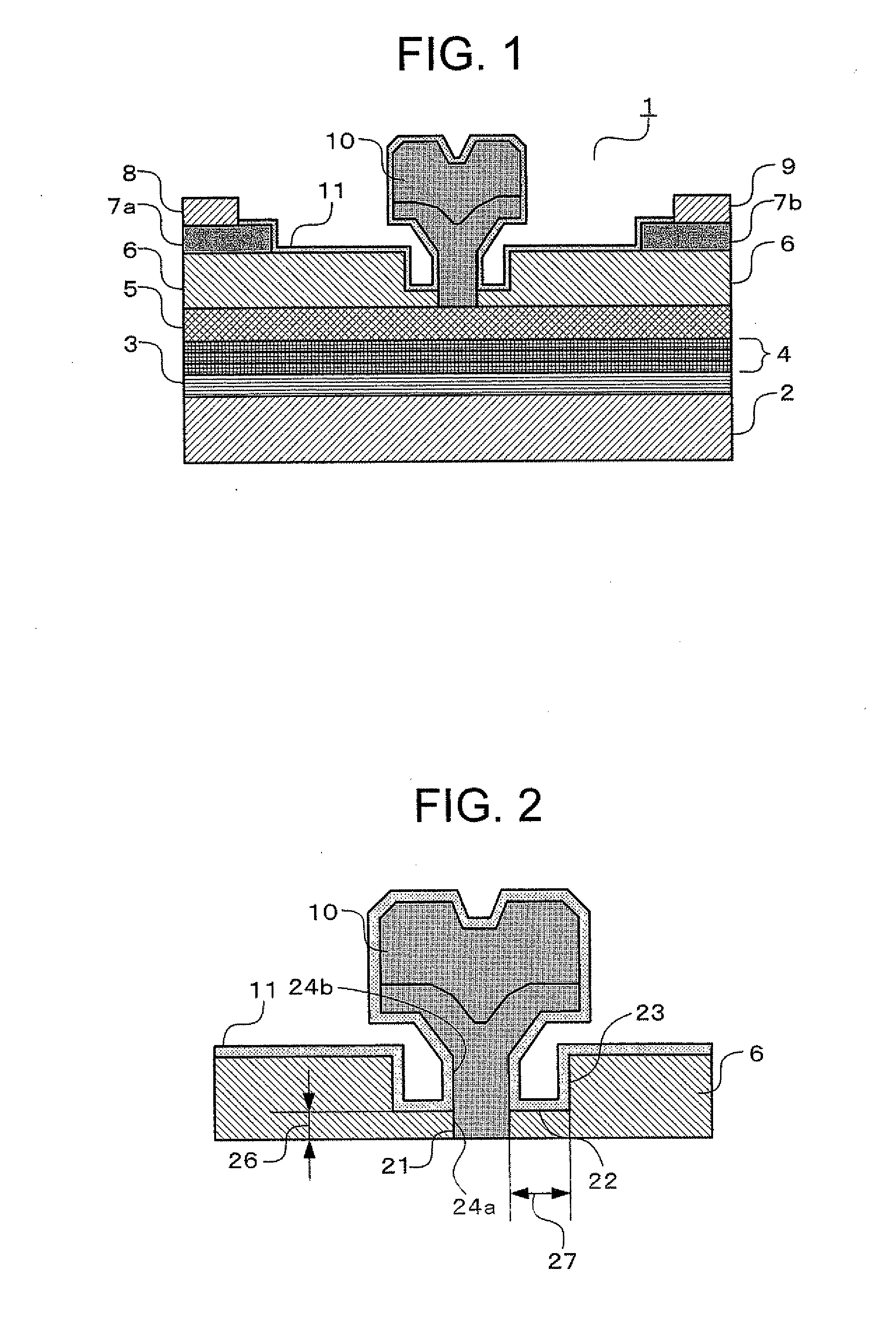
[0022]FIG. 1 is a sectional view of a field-effect transistor according to a first embodiment of the present invention. FIG. 2 is an enlarged sectional view of a periphery of a gate electrode.

[0023]A compound semiconductor according to the present invention corresponds to a III-V compound semiconductor. In addition to GaAs and GaN, gallium phosphide (GaP), gallium antimonide (GaSb), indium nitride (InN), and indium phosphide (InP) can also be used as the compound semiconductor. Further, as a semi-insulating substrate, a substrate composed of the GaAs or InP can be used.

[0024]Hereinafter, description will be made using the GaAs as an example of the III-V compound semiconductor.

[0025]As shown in FIG. 1, a field-effect transistor 1 according to a first embodiment of the present invention includes a buffer layer 3, a channel layer 4, a gate contact layer 5, and a gate buried layer 6. The buffer layer 3 is formed of an undoped GaAs epitaxial layer grown on a semi-insulating GaAs substrat...

second embodiment

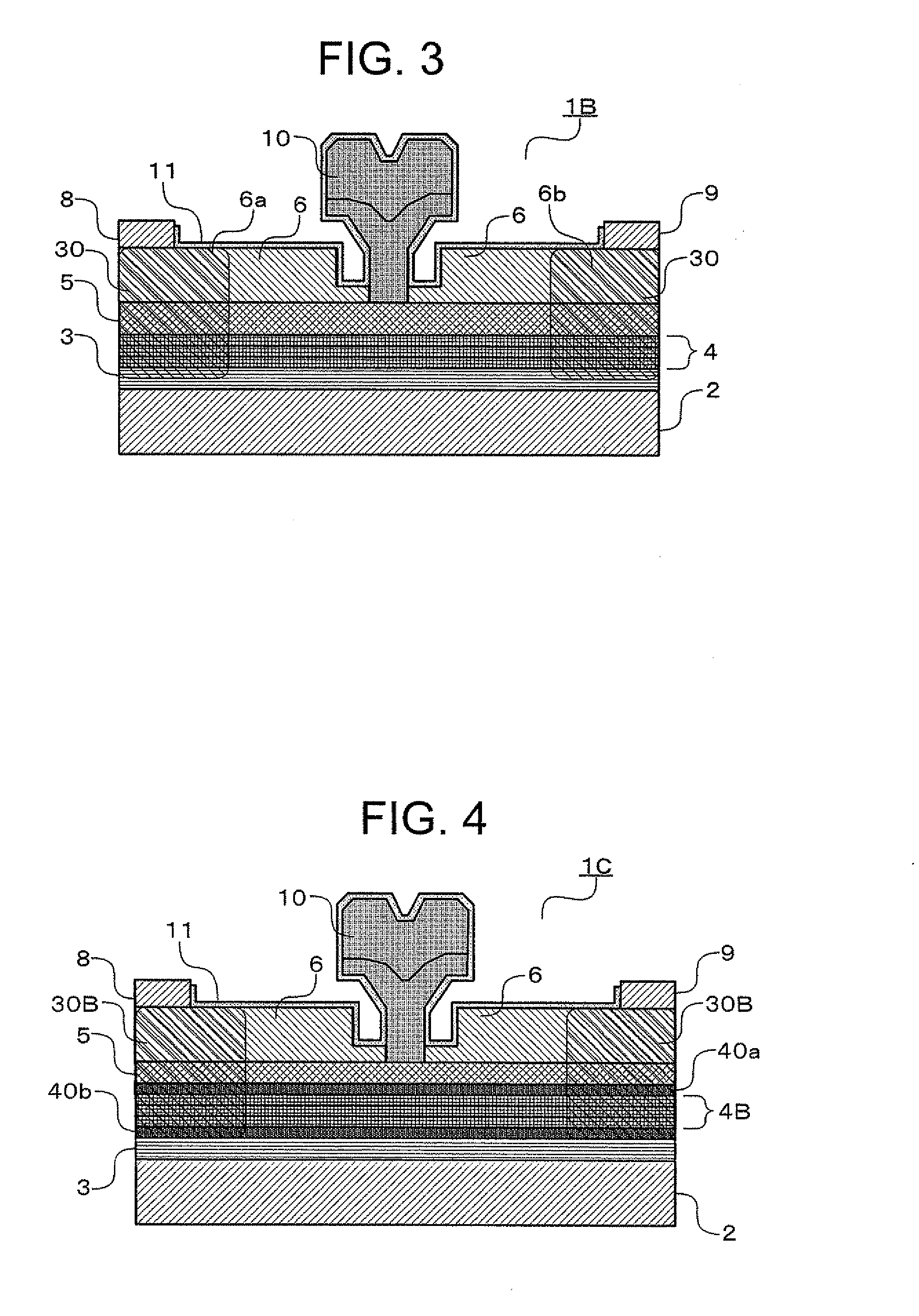
[0046]FIG. 3 is a sectional view of a field-effect transistor according to a second embodiment of the present invention.

[0047]A field-effect transistor 1B according to the second embodiment of the present invention is different from the field-effect transistor 1 according to the first embodiment in that the field-effect transistor 1B includes injection / anneal regions 30 in parts of a gate buried layer 6, a gate contact layer 5, and a channel layer 4 and does not include cap layers 7a and 7b. The other components of the field-effect transistor 1B are the same as those of the field-effect transistor 7 of the first embodiment, so the same components are denoted by the same reference numerals and the description thereof will be omitted.

[0048]As shown in FIG. 3, in the field-effect transistor 1B according to the second embodiment, regions 6a and 6b in the gate buried layer 6 and the injection / anneal regions 30 are formed. On the regions 6a and 6b, a source electrode 8 and a drain electro...

third embodiment

[0058]FIG. 4 is a sectional view of a field-effect transistor according to a third embodiment of the present invention.

[0059]A field-effect transistor 1C according to the third embodiment of the present invention is different from the field-effect transistor 1B according to the second embodiment in that the field-effect transistor 1C includes electron supply layers 40a and 40b and a channel layer 4B instead of the channel layer 4. The other components of the field-effect transistor 1C are the same as those of the field-effect transistor 1B of the second embodiment, so the same components are denoted by the same reference numerals and the description thereof will be omitted.

[0060]As shown in FIG. 4, the field-effect transistor 1C according to the third embodiment is a high electron mobility field-effect transistor (HEMT). The channel layer 4B is formed of an undoped InGaAs epitaxial layer in which conduction electrons move. Further, the field-effect transistor 1C according to the thi...


PUM


Abstract

A field-effect transistor includes a channel layer formed of a III-V compound semiconductor excluding aluminum; a gate contact layer formed of a III-V compound semiconductor and provided on the channel layer, the III-V compound semiconductor having a dopant concentration equal to or less than 1×1016 cm−3, containing aluminum, and having a large band gap energy; a gate buried layer of a III-V compound semiconductor and provided on the gate contact layer; and a gate electrode buried in the gate buried layer and in contact with the gate contact layer. A recess in the gate buried layer is opposed to an upper side wall of the gate electrode with a gap therebetween and a part of the gate buried layer, and where a contact with a lower side wall of the gate electrode is established, part of the gate buried layer remains without being removed.

Description

FIELD-EFFECT TRANSISTORBACKGROUND OF THE INVENTION[0001]1. Field of the Invention[0002]The present invention generally relates to a field-effect transistor using a compound semiconductor, which is suited to be used in a high frequency band of equal to or more than 800 MHz.[0003]2. Description of the Related Art[0004]A field-effect transistor using a compound semiconductor is generally used for a transmission / reception portion for a high speed / high capacity wireless communication system to amplify a high frequency signal of equal to or more than 800 MHz or to perform switching. An important characteristic required for a high frequency amplifier is a high output characteristic. In order to realize the high output in the high frequency band, it is effective to increase a maximum drain current or attain a high breakdown voltage.[0005]In general, an increase in a doped concentration for increasing the maximum drain current reduces the breakdown voltage. That is, the increase in the maxim...

Claims


Application Information

Patent Timeline
Patent Type & Authority Applications(United States)
IPC IPC(8): H01L29/74
CPCH01L29/2003H01L29/7787H01L29/42316H01L21/18
Inventor AMASUGA, HIROTAKAKUNII, TETSUO
Owner MITSUBISHI ELECTRIC CORP
Why Eureka
Try Eureka