Nonvolatile semiconductor memory device, semiconductor device and manufacturing method of nonvolatile semiconductor memory device

Active Publication Date: 2007-01-25
KIOXIA CORP
View PDF17 Cites 50 Cited by
  • Summary
  • Abstract
  • Description
  • Claims
  • Application Information

AI Technical Summary

Benefits of technology

[0009] An object of this invention is to form a tunnel insulating film of a nonvolatile semiconductor memory dev

Problems solved by technology

As a result, defects called traps are formed in the tunnel insulating film.
Therefore, a leak current increases and the data holding characteristic will be deteriorated.
However, in the process using NH3 gas, for example, an after-heat treatment at high temperatures is required to securely maintain the high reliability since a large amount of hydrogen is introduced in the tunnel insulating film.
Further, in a process using NO or N2O gas, there occurs a problem wh

Method used


Image

  • Nonvolatile semiconductor memory device, semiconductor device and manufacturing method of nonvolatile semiconductor memory device
  • Nonvolatile semiconductor memory device, semiconductor device and manufacturing method of nonvolatile semiconductor memory device
  • Nonvolatile semiconductor memory device, semiconductor device and manufacturing method of nonvolatile semiconductor memory device

Examples


Example

[0054] (First Embodiment)

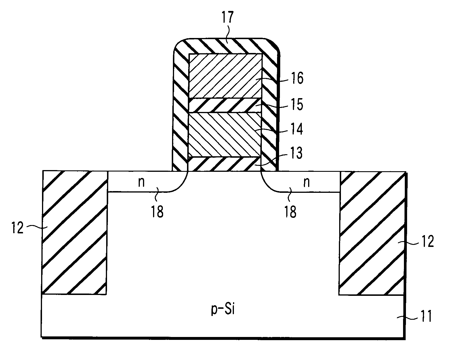
[0055]FIG. 1 is a cross sectional view showing the schematic structure of a nonvolatile semiconductor memory device according to a first embodiment of this invention.

[0056] A silicon thermal oxide film (element isolation insulating film) 12 for element isolation is embedded in and formed on a p-type (first conductivity type) silicon substrate (semiconductor substrate) 11 to surround the element forming area of the main surface of the substrate 11. On the main surface of the silicon substrate 11, a floating gate electrode 14 is formed with a tunnel insulating film (first gate insulating film) 13 disposed therebetween. On the floating gate electrode 14, a control gate electrode 16 is formed with an inter-poly insulating film (second gate insulating film) 15 disposed therebetween.

[0057] The inter-poly insulating film 15 is an ONO film with a thickness of 7 nm formed of a silicon oxide film, CVD silicon nitride film and CVD silicon oxide film, for example. Th...

Example

[0078] (Second Embodiment)

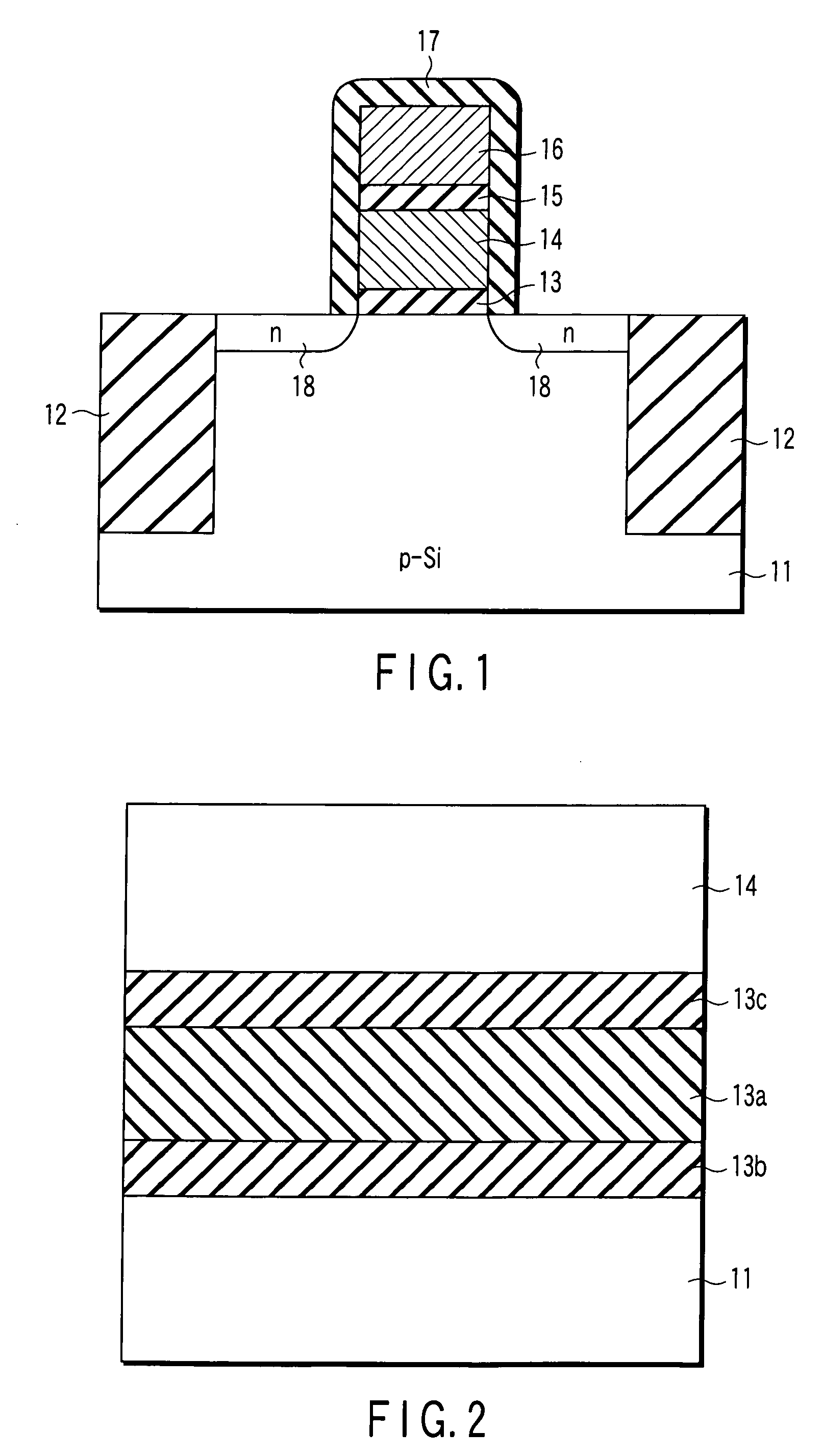
[0079]FIGS. 12A to 12E are cross sectional views showing a manufacturing process of a nonvolatile semiconductor memory device according to a second embodiment of this invention, and particularly, a manufacturing process of a tunnel insulating film. Portions which are the same as those of FIG. 1 are denoted by the same reference symbols and the detail explanation thereof is omitted.

[0080] First, as shown in FIG. 12A, the surface of a silicon substrate 11 is oxidized by use of oxygen gas, for example, to form a silicon oxide film 13b with a thickness of approximately 2 nm. Then, as shown in FIG. 12B, for example, a flat amorphous silicon film 13d with a thickness of approximately 1 nm is formed on the silicon oxide film 13b by use of disilane gas.

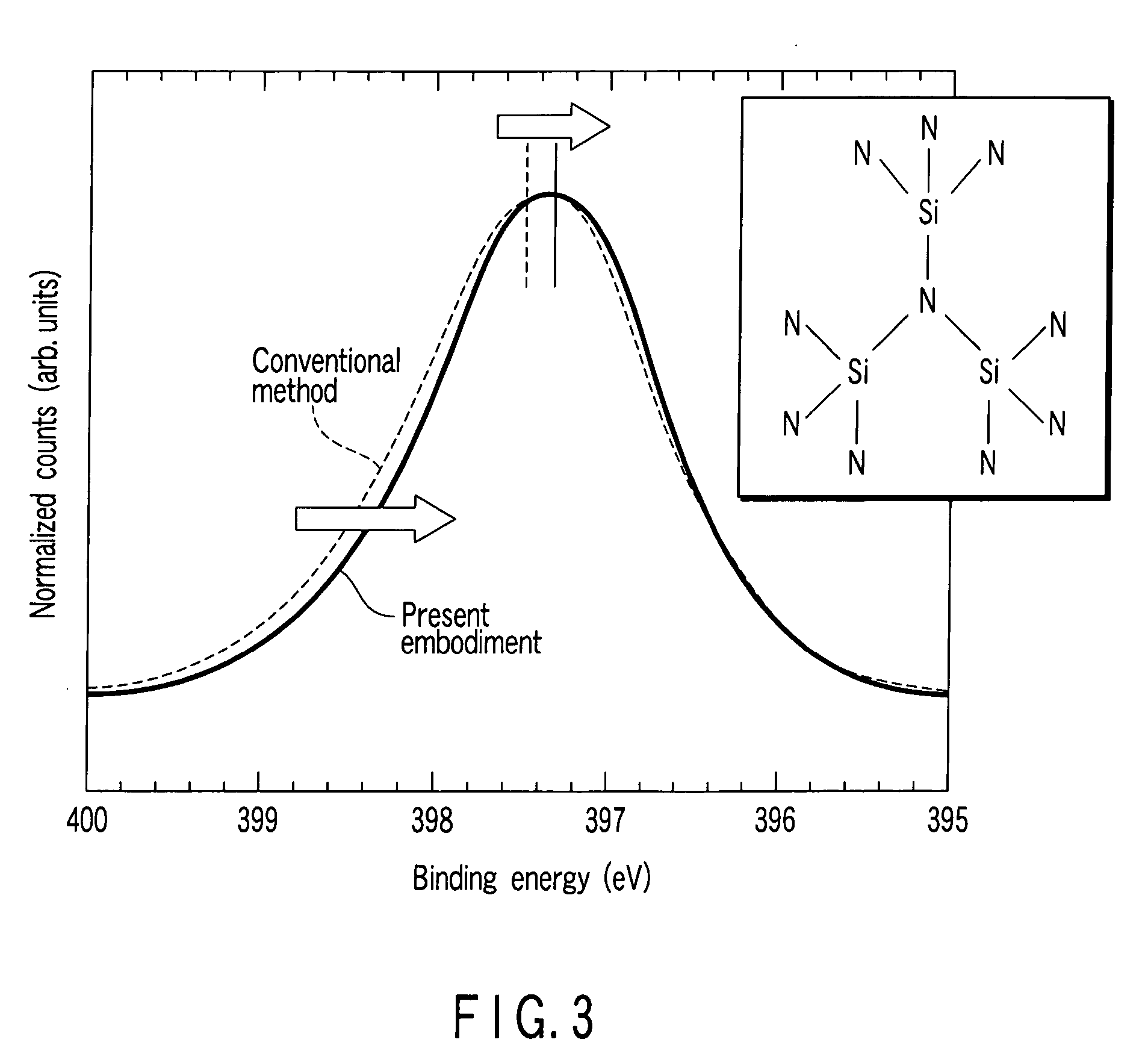
[0081] Next, as shown in FIG. 12C, the amorphous silicon film 13d is directly nitrided at a temperature of 700° C. under a pressure of 50 Torr (6650 Pa) by using a plasma nitriding method, for example. Thus, a sil...

Example

[0094] (Third Embodiment)

[0095]FIGS. 16A to 16I are cross sectional views showing the manufacturing process of a nonvolatile semiconductor memory device according to a third embodiment of this invention. Portions which are the same as those of FIG. 1 are denoted by the same reference symbols and the detail explanation thereof is omitted.

[0096] First, as shown in FIG. 16A, for example, a p-type (first conductivity type) silicon substrate 11 having plane orientation (100) and resistivity 10 to 20 Ωcm is prepared and a groove is formed in the surface of the silicon substrate 11. An element isolation insulating film 12 with a thickness of approximately 0.6 μm is formed by burying a CVD oxide film in the groove. Then, an oxidizing process is performed at 950° C. by use of oxygen gas to form a silicon oxide film 13b with a thickness of approximately 2 nm on the surface of the silicon substrate 11. Next, for example, an amorphous silicon film 13d of approximately 1.5 nm is deposited at 4...


PUM


Abstract

A nonvolatile semiconductor memory device includes a gate portion formed by laminating a tunnel insulating film, floating gate electrode, inter-poly insulating film and control gate electrode on a semiconductor substrate, and source and drain regions formed on the substrate. The tunnel insulating film has a three-layered structure having a silicon nitride film sandwiched between silicon oxide films. The silicon nitride film is continuous in an in-plane direction and has 3-coordinate nitrogen bonds and at least one of second neighboring atoms of nitrogen is nitrogen.

Description

CROSS-REFERENCE TO RELATED APPLICATIONS [0001] This application is based upon and claims the benefit of priority from prior Japanese Patent Applications No. 2005-214613, filed Jul. 25, 2005; and No. 2006-123914, filed Apr. 27, 2006, the entire contents of both of which are incorporated herein by reference. BACKGROUND OF THE INVENTION [0002] 1. Field of the Invention [0003] This invention relates to a nonvolatile semiconductor memory device with a stacked gate structure having a floating gate electrode and control gate electrode stacked on a semiconductor substrate and a manufacturing method thereof. Further, this invention relates to a semiconductor device having a gate electrode formed on a semiconductor substrate with a gate insulating film disposed therebetween. [0004] 2. Description of the Related Art [0005] Recently, miniaturization of elements is rapidly advanced in an electrically programmable and erasable nonvolatile semiconductor memory (EEPROM). In the EEPROM, high voltage...

Claims


Application Information

Patent Timeline
IPC IPC(8): H01L29/788H01L21/336
CPCH01L21/28273H01L27/115H01L27/11521H01L29/7881H01L29/513H01L29/785H01L29/42332H01L29/40114H10B69/00H10B41/30H01L21/3213
Inventor MITANI, YUUICHIROMATSUSHITA, DAISUKEOOBA, RYUJIKAMIOKA, ISAOOZAWA, YOSHIO
Owner KIOXIA CORP
Why Eureka
Try Eureka