Chip design method and device, chip, electronic equipment and storage medium

A chip design, chip technology, applied in design optimization/simulation, special data processing applications, etc., can solve problems such as lack of design methods for custom computing chips in the field

Active Publication Date: 2021-11-26
WUXI RES INST OF APPLIED TECH TSINGHUA UNIV
View PDF3 Cites 1 Cited by
  • Summary
  • Abstract
  • Description
  • Claims
  • Application Information

AI Technical Summary

Problems solved by technology

[0003] Due to the increasing demand for computing power from application development and the increasing demand for energy efficiency from process development, the design methods of general-purpose computing chips are facing huge challenges. Domain-customized computing has become a popular direction in chip design, but domain-customized computing chips are still lacking effective solutions. Design method guidance, relying on experience exploration and continuous iteration of senior designers

Method used


Image

  • Chip design method and device, chip, electronic equipment and storage medium
  • Chip design method and device, chip, electronic equipment and storage medium
  • Chip design method and device, chip, electronic equipment and storage medium

Examples


Embodiment Construction

[0055] In order to make the purpose, features and advantages of the present invention more obvious and understandable, the technical solutions in the embodiments of the present invention will be clearly and completely described below in conjunction with the accompanying drawings in the embodiments of the present invention. Obviously, the described The embodiments are only some of the embodiments of the present invention, but not all of them. Based on the embodiments of the present invention, all other embodiments obtained by those skilled in the art without making creative efforts belong to the protection scope of the present invention.

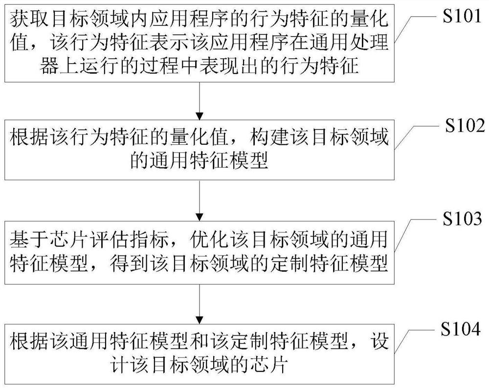
[0056] The present invention provides a chip design method, including: obtaining the quantified value of the behavioral characteristics of the application program in the target field, the behavioral characteristics representing the behavioral characteristics of the application program in the process of running on a general processor; according...


PUM


Abstract

The invention discloses a chip design method, and is applied to the technical field of chip design, the method comprises the following steps: obtaining a quantized value of a behavior characteristic of an application program in a target field, the behavior characteristic representing the behavior characteristic of the application program in a process of running on a universal processor; constructing a general feature model of the target domain according to the quantized value of the behavior feature; based on the chip evaluation index, optimizing the general feature model of the target domain to obtain a customized feature model of the target domain; and designing a chip of the target domain according to the general feature model and the customized feature model. The invention also discloses a chip design device, a chip, electronic equipment and a storage medium, the method is different from a design method of a general computing chip and a design method of a special computing chip, is oriented to chip design in a specific field, and can take both high flexibility and high energy efficiency into account.

Description

technical field [0001] The invention relates to the technical field of chip design, in particular to a chip design method, device, chip electronic equipment and storage medium. Background technique [0002] With the transformation and development of modern society in the direction of digitization, intelligence, and automation, a large number of emerging applications require far more computing power than ever before. Big data, cloud computing, artificial intelligence, and bioinformatics have become the most popular development fields, and the ability to process and analyze massive data has become the core ability to adapt to the development of an information society. [0003] Due to the increasing demand for computing power from application development and the increasing demand for energy efficiency from process development, the design methods of general-purpose computing chips are facing huge challenges. Domain-customized computing has become a popular direction in chip desi...

Claims


Application Information

Patent Timeline
IPC IPC(8): G06F30/20
CPCG06F30/20
Inventor 刘雷波朱建峰
Owner WUXI RES INST OF APPLIED TECH TSINGHUA UNIV
Why Eureka
Try Eureka