Silicon wafer classifying and collecting method

A silicon wafer and chip receiving technology, which is applied to conveyor control devices, conveyor objects, loading/unloading, etc., can solve the problem of low chip receiving efficiency

Pending Publication Date: 2021-11-30
WUXI AUTOWELL TECH
View PDF9 Cites 0 Cited by
  • Summary
  • Abstract
  • Description
  • Claims
  • Application Information

AI Technical Summary

Problems solved by technology

[0003] In the above-mentioned sorting film collection method, since the qualified films and all kinds of defective films need to be reversed and transported through the main conveying line, the receiving speed of qualified films and the film receiving speed of defective films are mutually restricted, so the overall film receiving efficiency lower

Method used


Image

  • Silicon wafer classifying and collecting method
  • Silicon wafer classifying and collecting method
  • Silicon wafer classifying and collecting method

Examples


no. 1 approach

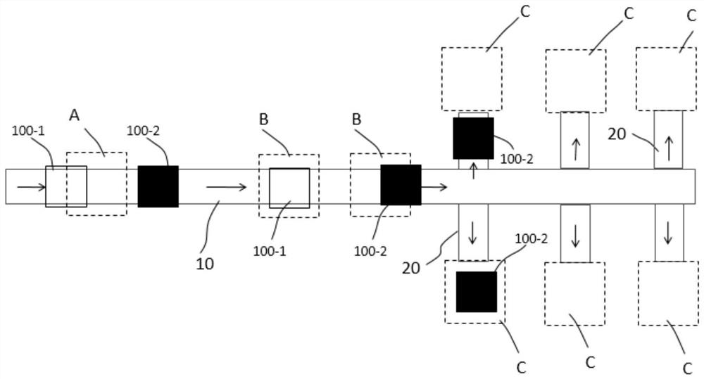
[0056] like figure 2 As shown, in this embodiment, the first type of silicon wafer 100-1 is transported to the first receiving station B by using the first conveying device 10 to implement the receiving of the first type of silicon wafer 100-1, including:

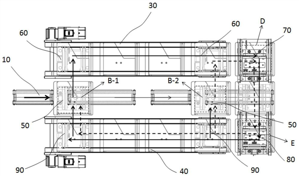
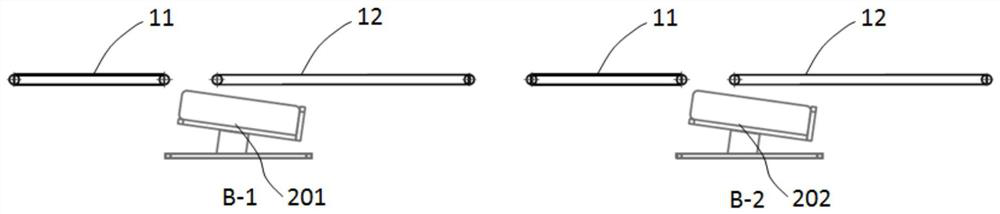
[0057] The first type of silicon wafer 100 - 1 is transported to the magazine located at the first receiving station B by the first transport device 10 . optional, figure 2 In the embodiment, there are two first film receiving stations, respectively the first film receiving station B-1 and the first film receiving station B-2, and the first type of silicon wafer 100-1 is received to In the magazine at the first film receiving station B-1 or the first film receiving station B-2, of course, in other embodiments, one, three, etc. other numbers of first film receiving stations can also be set .

[0058] After the magazine at the first film receiving station B-1 or the first film receiving station B-2 is filled with the fir...

no. 2 approach

[0094] Continuing the description in the first embodiment: after the magazine at the first film receiving station is filled with the first type of silicon wafers 100-1, the full magazine is removed from the first film receiving station and transported to the A receiving station D on the first side of the film receiving station.

[0095] However, when there is currently a stranded full box at the receiving station D, the full box that is currently filled with the first type of silicon wafer 100-1 cannot be directly transported from the first receiving station where it is located to the receiving station. D, thus causing the film to wait.

[0096] In order to solve this problem, a full box buffer station is also provided in this embodiment.

[0097] After the magazine at the first receiving station is full of the first type of silicon wafers 100-1, it is first detected whether there is a magazine at the receiving station D. When there is currently a magazine at the receiving s...

no. 3 approach

[0107] In this embodiment, the silicon wafers of the first type are qualified silicon wafers whose test results meet the predetermined standard, and the silicon wafers of the second type are unqualified silicon wafers whose test results do not meet the predetermined standard. As understood by those skilled in the art, different types of unqualified silicon wafers have different recycling methods. For example, silicon wafers with dirty surfaces may be converted into qualified silicon wafers after cleaning.

[0108] In view of this, according to the test results, the second-type silicon wafers 100-2 are further divided into several sub-categories. For example, the second type of silicon wafer 100-2 is further divided into three subcategories: silicon wafers with dirty surfaces, silicon wafers with holes on the surface, and silicon wafers with chipped edges.

[0109] In this embodiment, the second delivery device 20 transports the second type of silicon wafer 100-2 to the second ...


PUM


Abstract

The invention provides a silicon wafer classifying and collecting method. The silicon wafer classifying and collecting method comprises the steps that silicon wafers are conveyed by a first conveying device to a detection station; the silicon wafers are detected at the detection station, and the silicon wafers are divided into a first type of silicon wafers of which the detection result meets a predetermined standard and a second type of silicon wafers of which the detection result does not meet the predetermined standard according to the detection result; the first type of silicon wafers are conveyed by the first conveying device to a first wafer receiving station so as to receive the first type of silicon wafers; the second type of silicon wafers are transferred from the first conveying device to a second conveying device located on the side of the first conveying device; and the second type of silicon wafers are conveyed by the second conveying device to a second wafer receiving station so as to receive the second type of silicon wafers. According to the silicon wafer classifying and collecting method, the second type of silicon wafers are reversed to the second conveying device located on the side of the first conveying device to be collected, the first type of silicon wafers are directly collected on the first conveying device, therefore, the collecting processes of the two types of silicon wafers do not interfere with each other, and finally the overall collecting efficiency is improved.

Description

technical field [0001] The invention relates to the field of battery production, in particular to a method for sorting and receiving silicon wafers. Background technique [0002] Before the silicon wafers are made into cells, it is first necessary to complete the inspection of the silicon wafers, and then classify and receive the silicon wafers according to the inspection results. In the traditional method of sorting and receiving silicon wafers, the silicon wafers are inspected first, and the inspected silicon wafers are transported to the rear channel through the main conveying line. , All kinds of defective sheets are reversed and transported to the corresponding material boxes on both sides of the main conveying line, which completes the process of conveying and collecting the sheets on the main conveying line. [0003] In the above-mentioned sorting film collection method, since the qualified films and all kinds of defective films need to be reversed and transported th...

Claims


Application Information

Patent Timeline
IPC IPC(8): B65G15/24B65G43/08B65G47/46B65G65/32
CPCB65G15/24B65G43/08B65G47/46B65G65/32Y02P70/50
Inventor 刘世挺李文谭晓靖葛建良李昶王美徐飞赵铭李泽通薛冬冬
Owner WUXI AUTOWELL TECH
Why Eureka
Try Eureka