Touch substrate and touch display device
A substrate and touch technology, applied in instruments, computing, electrical and digital data processing, etc., can solve problems such as excessively long metal traces and reduce product yield, and achieve the goal of preventing ESD, improving yield, and reducing static electricity accumulation. Effect
- Summary
- Abstract
- Description
- Claims
- Application Information
AI Technical Summary
Problems solved by technology
Method used
Image


Examples
Embodiment Construction
[0041] In order to make the purpose, technical solutions and advantages of the present invention more clear, the touch substrate and the touch display device provided by the embodiments of the present invention will be further described in detail below in conjunction with the accompanying drawings. Obviously, the described embodiments are only examples of the present invention. Some, but not all, embodiments. Based on the embodiments of the present invention, all other embodiments obtained by persons of ordinary skill in the art without making creative efforts belong to the protection scope of the present invention.
[0042] The shapes and sizes of the components in the drawings do not reflect the real scale, but are only intended to schematically illustrate the content of the present invention.
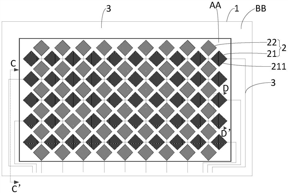
[0043] An embodiment of the present invention provides a touch substrate, such as Figure 1-Figure 3 as shown, figure 1 is a schematic plan view of the touch substrate, figure 2 ...
PUM
 Abstract
Description
Claims
Application Information