FLASH chip programming method and device and electronic equipment
An electronic device and chip technology, applied in software engineering design, electrical digital data processing, software deployment, etc., can solve the problems of complicated operation process and low programming efficiency, and achieve the effect of simplifying the operation process and improving the programming efficiency.
- Summary
- Abstract
- Description
- Claims
- Application Information
AI Technical Summary
Problems solved by technology
Method used
Image

Examples
Embodiment 1
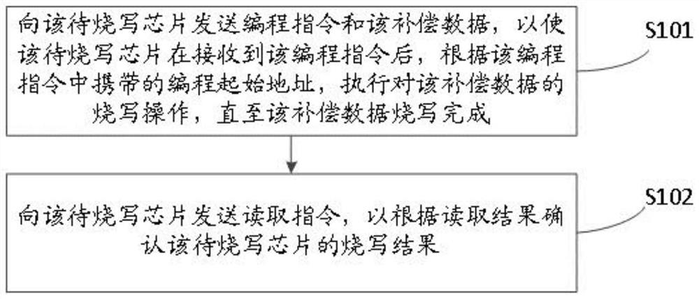
[0031] like figure 1 As shown, a schematic flow chart of a FLASH chip programming method is provided for an embodiment of the present invention. The method is applied to a display driver chip, and the display driver chip is connected to the chip to be programmed; the chip to be programmed is used to store the corresponding display screen Compensation data for display defects; the method includes:
[0032] Step S101: Send the programming instruction and the compensation data to the chip to be programmed, so that after the chip to be programmed receives the programming instruction, it executes programming of the compensation data according to the programming start address carried in the programming instruction. Programming operation until the compensation data programming is completed.
[0033] In this embodiment, the display driver chip starts the programming operation, and then sends the programming instruction and the compensation data to the chip to be programmed. Wherein,...
Embodiment 2
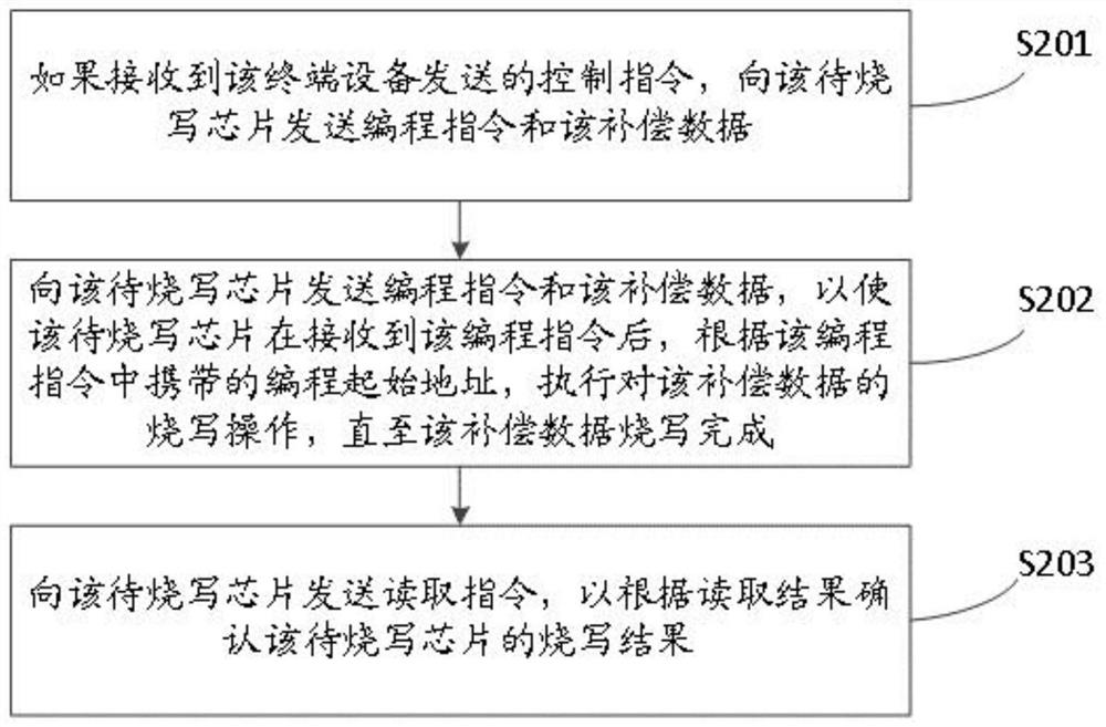
[0039] exist figure 1 On the basis of the above, this embodiment also provides another FLASH chip programming method, which is applied to a display driver chip, and the display driver chip is connected to the chip to be programmed; the chip to be programmed is used to store the corresponding display screen Displays compensation data for defects. Wherein, the display screen is an active matrix organic light emitting diode or an active matrix organic light emitting diode screen.
[0040] figure 2 A schematic flow chart of another FLASH chip programming method is provided for the embodiment of the present invention, wherein the display driver chip is connected to the terminal device, and the method consists of figure 2 see:
[0041] Step S201: If the control instruction sent by the terminal device is received, send the programming instruction and the compensation data to the chip to be programmed.
[0042] In this embodiment, the terminal device is a host computer with a pr...
Embodiment 3
[0054] The embodiment of the present invention also provides a FLASH chip programming device, such as Figure 5 As shown, a schematic diagram of a FLASH chip programming device is provided for an embodiment of the present invention, wherein the device is applied to a display driver chip, and the display driver chip is connected to the chip to be programmed; the chip to be programmed is used to store the corresponding display Compensation data for display defects of the screen; the device includes:
[0055] The programming start module 51 is used to send a programming instruction and the compensation data to the chip to be programmed, so that after the chip to be programmed receives the programming instruction, it executes according to the programming start address carried in the programming instruction. The programming operation of the compensation data is performed until the programming of the compensation data is completed.
[0056] The programming and reading module 52 is ...
PUM
 Abstract
Description
Claims
Application Information
 - R&D
- Intellectual Property
- Life Sciences
- Materials
- Tech Scout
- Unparalleled Data Quality
- Higher Quality Content
- 60% Fewer Hallucinations
Browse by: Latest US Patents, China's latest patents, Technical Efficacy Thesaurus, Application Domain, Technology Topic, Popular Technical Reports.
© 2025 PatSnap. All rights reserved.Legal|Privacy policy|Modern Slavery Act Transparency Statement|Sitemap|About US| Contact US: help@patsnap.com