Supercharge Your Innovation With Domain-Expert AI Agents!

Semiconductor package device

A packaging device and semiconductor technology, which is applied in the direction of semiconductor devices, semiconductor/solid-state device parts, electric solid-state devices, etc., can solve the problems of insufficient internal space of the package body and the inability to use small semiconductor chips in the voltage regulator, and achieve the goal of reducing space Effect

Pending Publication Date: 2021-12-17
NAN YA TECH
View PDF0 Cites 0 Cited by
  • Summary
  • Abstract
  • Description
  • Claims
  • Application Information

AI Technical Summary

Problems solved by technology

[0003] In the field of semiconductor packaging, voltage regulators cannot be used in semiconductor packaging devices with small semiconductor chips due to insufficient space inside the package
Therefore, small-sized semiconductor chips with high power consumption are negatively affected by external power and self-noise

Method used


Image

  • Semiconductor package device
  • Semiconductor package device
  • Semiconductor package device

Examples


Embodiment Construction

[0030] The invention can be embodied in many different forms. Representative embodiments are shown in the drawings and described in detail herein. The present disclosure contains examples or illustrations of principles, and the disclosed embodiments of the invention are not to be limited to the illustrated embodiments.

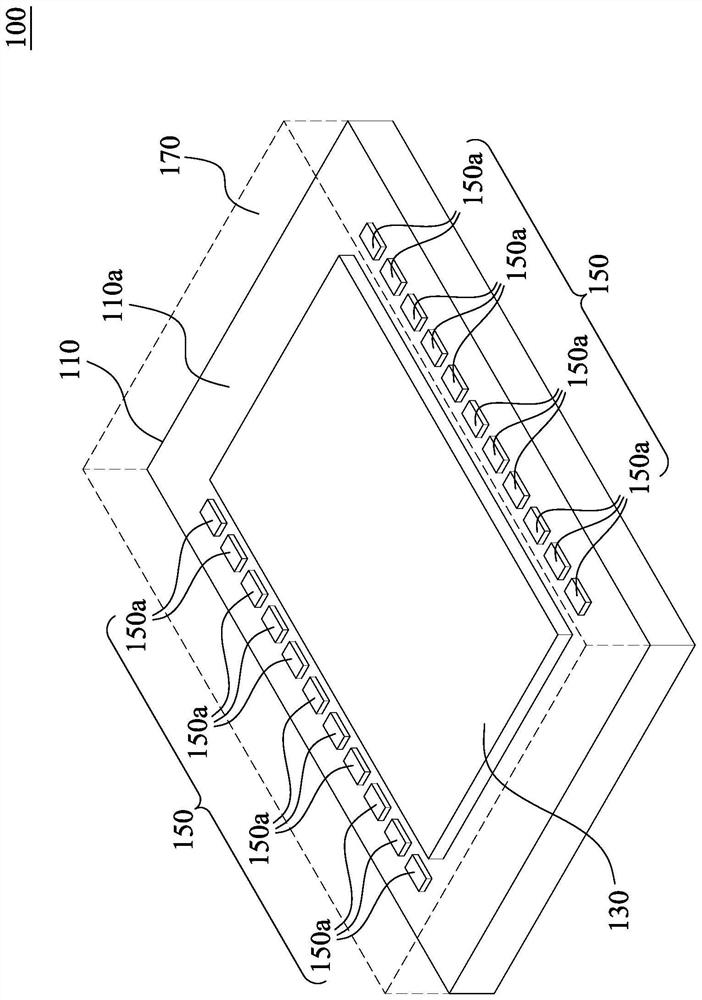
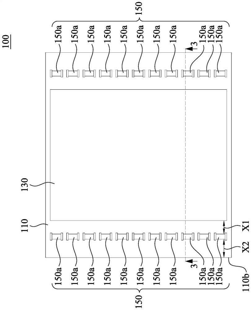
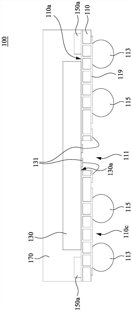
[0031] Please refer to Figure 1 to Figure 4 . figure 1 It is a three-dimensional schematic view of the semiconductor packaging device 100 . figure 2 shown as figure 1 , a schematic top view of the semiconductor packaging device 100 . image 3 shown as figure 2 , the cross-sectional view of the semiconductor package device 100 is drawn along the section line 3-3. Figure 4 shown as figure 1 , a circuit diagram of the semiconductor package device 100 . In one embodiment of the present invention, the semiconductor package device 100 includes a substrate 110 , a memory chip 130 , and a decoupling array 150 . The substrate 110 has an upper surface 110a,...


PUM


Abstract

The invention discloses a semiconductor package device which includes a substrate, a memory chip, and a decoupling array. The substrate has a top surface, a power end, and a grounding end. The memory chip is located on the top surface of the substrate and has a power pad in which the power pad is electrically connected to the power end at a node to receive electric power. A decoupling array is located on the top surface of the substrate, and the decoupling array has a plurality of decoupling capacitors connected in parallel. Each decoupling capacitor is electrically connected between the node and the grounding end so as to shunt power transmitted from the power supply terminal to the memory chip.

Description

technical field [0001] The invention relates to a semiconductor packaging device. More specifically, it refers to a semiconductor package device capable of regulating input power. Background technique [0002] In the development of technology related to semiconductor chips, the reduction of chip size is the main trend. As the demand for semiconductor chips increases rapidly, the space for accommodating internal components is gradually reduced. [0003] In the field of semiconductor packaging, voltage regulators cannot be applied to semiconductor packaging devices with small semiconductor chips due to insufficient space inside the package. Therefore, small-sized semiconductor chips with high power consumption are negatively affected by external power and self-noise. [0004] From the above description, it can be seen that it is necessary to develop a semiconductor packaging device to achieve volume reduction while regulating external power and reducing the negative impact ...

Claims


Application Information

Patent Timeline
Patent Type & Authority Applications(China)
IPC IPC(8): H01L23/64H01L23/31
CPCH01L23/642H01L23/3107H01L23/3128H01L25/16H01L23/50H01L23/49816H01L23/13H01L23/49822H01L2924/15311H01L2924/15151H01L2224/4824H01L2924/19041H01L2924/19105H01L2224/04042H01L24/48H01L23/49838H01L28/40
Inventor 杨吴德
Owner NAN YA TECH
Features
  • R&D
  • Intellectual Property
  • Life Sciences
  • Materials
  • Tech Scout
  • Unparalleled Data Quality
  • Higher Quality Content
  • 60% Fewer Hallucinations
Learn More