FPGA-based fast data information sorting method and system, equipment and storage medium
A technology of quick sorting and data information, applied in data classification, processing input data, etc., can solve the problems that cannot be sorted into dynamic storage problems, can not greatly reduce resource usage, sorting efficiency, etc., to reduce resource usage , improve sorting efficiency, improve the effect of operating efficiency
- Summary
- Abstract
- Description
- Claims
- Application Information
AI Technical Summary
Problems solved by technology
Method used
Image

Examples
Embodiment 1
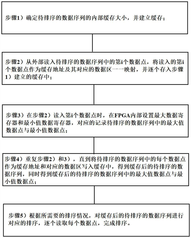
[0061] figure 2 The correspondence between the address and the data area sorted without duplicate data sequence array;
[0062] For the data sequence to be sorted, it is recorded as the array {2, 10, 8, 3, 9, 5, 7, 4}, according to step 1), the cache width is 1bit, the cache depth is 10 storage area, as Cache; When power-on, initialize all data regions within the cache to 0. When the arrangement array is entered, according to step 2), the first data point data 2 is read from the outside, which is written as the cache address 2, and the cache address 2 corresponds to 1, and the cache address 2 and data will be District 1 conducts mapping, and deposits the established cache, and sets the maximum value data register and the minimum value data register according to step 3) and writes 2; then repeat step 2), read the second data point from the outside Data 10, as a cache address, write the data area corresponding to the cache address 10 to 1, repeat step 3), update the maximum value d...
Embodiment 2
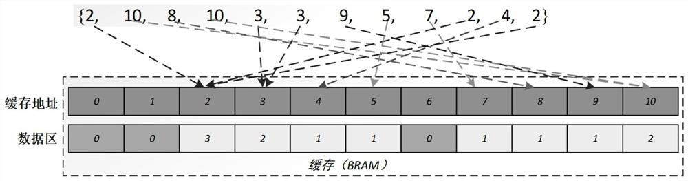
[0064] image 3 The correspondence between addresses and data areas are derived by repeated data sequence array;
[0065] For the data sequence to be sorted, it is recorded as the descending data {2, 10, 8, 10, 3, 3, 9, 5, 7, 2, 4, 2}, according to step 1), establish a cache width of 4BIT, cache The storage area of the depth is 10, as a cache, when power-on, initializes all data regions within the cache to 0. When the arrangement array is entered, according to step 2), the first data point data 2 is read from the outside, which is placed as the cache address 2; the data area corresponding to the read cache address 2 is placed in a temporary register. At this time the value is 0, add this value to 1, write back the data area corresponding to the cache address 2; simultaneously set the maximum value data register and the minimum value data register, and write 2; then repeat step 2) from the outside first read The second data point data 10 is used as the cache address, reads the da...
PUM
 Abstract
Description
Claims
Application Information
 - Generate Ideas
- Intellectual Property
- Life Sciences
- Materials
- Tech Scout
- Unparalleled Data Quality
- Higher Quality Content
- 60% Fewer Hallucinations
Browse by: Latest US Patents, China's latest patents, Technical Efficacy Thesaurus, Application Domain, Technology Topic, Popular Technical Reports.
© 2025 PatSnap. All rights reserved.Legal|Privacy policy|Modern Slavery Act Transparency Statement|Sitemap|About US| Contact US: help@patsnap.com