

Semiconductor light-emitting element
A light-emitting element and semiconductor technology, which is applied in the direction of semiconductor devices, electrical components, circuits, etc., can solve the problems of increased current density of the electrode layer and deterioration of the electrode layer, and achieve the effect of suppressing electromigration and suppressing the increase of driving voltage
- Summary
- Abstract
- Description
- Claims
- Application Information
AI Technical Summary
Problems solved by technology
Method used
Image


Examples
Embodiment approach
[0051] Hereinafter, embodiments of the present invention will be described with reference to the drawings. In addition, the embodiment described below shows a specific example of the present invention. Therefore, numerical values, shapes, materials, constituent elements, arrangement positions and connection forms of constituent elements, steps and the order of steps, etc. shown in the following embodiments are examples and are not intended to limit the present invention.
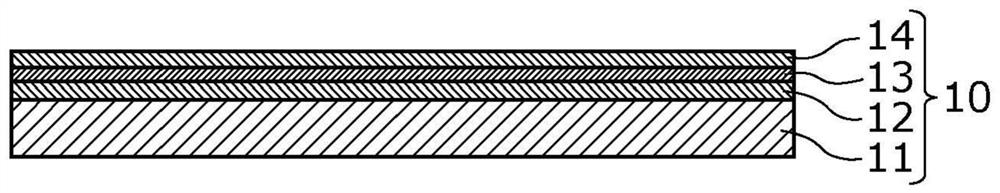
[0052] In addition, each drawing is a schematic diagram, and is not necessarily strictly illustrated. Therefore, scales and the like do not necessarily coincide in the respective drawings. In addition, in each figure, the same code|symbol is attached|subjected to the substantially same structure, and a repeated description is abbreviate|omitted or simplified.
Embodiment approach 1
[0054] [Semiconductor light emitting element]
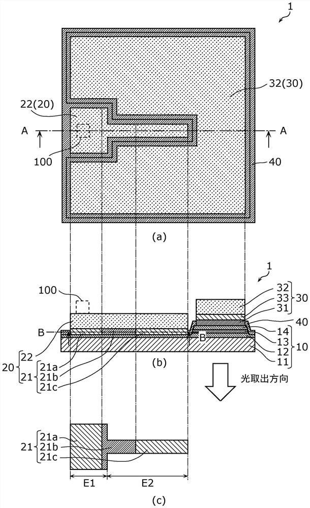
[0055] First, use figure 1 The structure of the semiconductor light emitting element 1 of Embodiment 1 will be described. exist figure 1 Among them, (a) is a plan view of the semiconductor light emitting element 1 of Embodiment 1, (b) is a vertical cross-sectional view of the semiconductor light emitting element 1 taken along line AA of (a), and (c) is a BB of (b) A horizontal cross-sectional view of the semiconductor light emitting element 1 of the line. In addition, in figure 1 In the plan view of (a), hatching is appropriately applied in order to facilitate understanding of the positional relationship between the components. This also applies to the following drawings.
[0056] Such asfigure 1 As shown, the semiconductor light emitting element 1 of Embodiment 1 has a semiconductor stacked structure 10 and an n-side electrode 20 and a p-side electrode 30 provided on the semiconductor stacked structure 10 . In this embodim...
Embodiment approach 2
[0217] Next, use Figure 22 A semiconductor light emitting element 1H of Embodiment 2 will be described. exist Figure 22 Among them, (a) is a plan view of the semiconductor light emitting element 1H according to Embodiment 2, (b) is a vertical cross-sectional view of the semiconductor light emitting element 1H taken along line AA of (a), and (c) is BB of (b) A horizontal cross-sectional view of the semiconductor light emitting element 1H of the line.
[0218] The semiconductor light emitting element 1H of the present embodiment is different from the semiconductor light emitting element 1 of the first embodiment described above in the structure of the n-side electrode 20H.
[0219] Specifically, in the semiconductor light emitting element 1 of Embodiment 1 above, the n-side electrode layer 21 of the n-side electrode 20 has the first metal layer 21a, the second metal layer 21b, and the third metal layer 21c, but in this embodiment of the semiconductor light emitting element ...
PUM
| Property | Measurement | Unit |
|---|---|---|
| Film thickness | aaaaa | aaaaa |
| Film thickness | aaaaa | aaaaa |
| Film thickness | aaaaa | aaaaa |
Abstract
Description
Claims
Application Information