Manufacturing method of semiconductor device

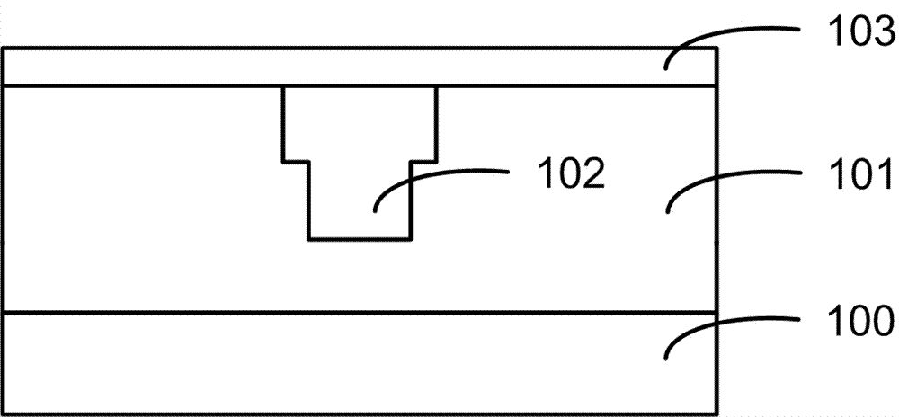
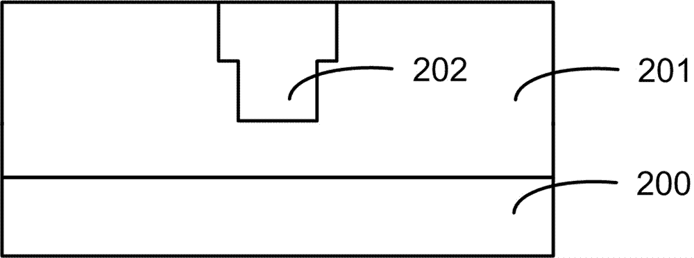
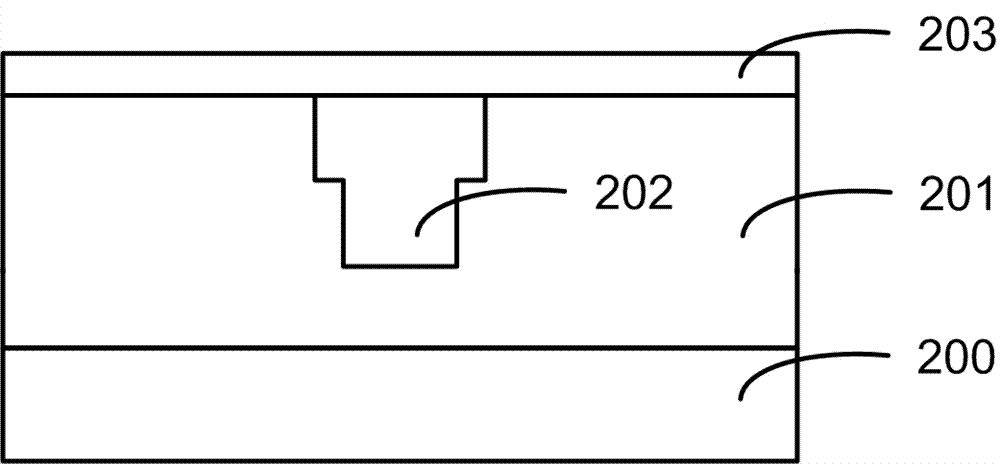
A manufacturing method and semiconductor technology, applied in semiconductor/solid-state device manufacturing, electrical components, circuits, etc., can solve the problems of reduced barrier capacity, shortened electromigration life of metal interconnection lines 102, and fracture of copper interconnection structures, etc., to achieve extended Effect of electromigration life, suppression of electromigration phenomenon, and reliability assurance

Inactive Publication Date: 2013-01-30
SEMICON MFG INT (SHANGHAI) CORP
View PDF4 Cites 3 Cited by
  • Summary
  • Abstract
  • Description
  • Claims
  • Application Information

AI Technical Summary

Problems solved by technology

As we all know, electromigration is one of the important factors affecting the reliability of metal interconnection. Electromigration may lead to thinning of metal interconnection, increase its resistivity, and even cause the copper interconnection structure to break.
In addition, in order to further reduce the dielectric constant, one of the research directions is to increase the porosity in the dielectric material. It is conceivable that this will further reduce the barrier ability of the cap layer 103 to moisture and oxygen, so that the cap layer 103 covers The electromigration (Electro Migration, EM) phenomenon in the metal interconnection 102 is more serious, and the electromigration life of the metal interconnection 102 is seriously shortened, which affects the reliability of the semiconductor device

Method used


Image

  • Manufacturing method of semiconductor device
  • Manufacturing method of semiconductor device
  • Manufacturing method of semiconductor device

Examples


Embodiment Construction

[0020] Next, the present invention will be described more completely with reference to the accompanying drawings, in which embodiments of the present invention are shown. However, the present invention can be implemented in different forms and should not be construed as being limited to the embodiments presented here. On the contrary, the provision of these embodiments will make the disclosure thorough and complete, and will fully convey the scope of the present invention to those skilled in the art. In the drawings, the sizes and relative sizes of layers and regions may be exaggerated for clarity. The same reference numerals denote the same elements throughout.

[0021] It should be understood that when an element or layer is referred to as being "on", "adjacent to", "connected to" or "coupled to" other elements or layers, it can be directly on the other elements or layers. On a layer, adjacent to, connected or coupled to other elements or layers, or intervening elements or la...


PUM

PropertyMeasurementUnit
thicknessaaaaaaaaaa

Abstract

The invention discloses a manufacturing method of a semiconductor device. The method includes the steps: a) providing a semiconductor substrate, forming a dielectric layer on the semiconductor substrate and a metal interconnection line inlaid in the dielectric layer; b) forming an ultrathin silicon nitride layer on the metal interconnection line and the dielectric layer; and c) forming a cap layer on the ultrathin silicon nitride layer. Since the silicon nitride layer excellent in sealability is formed between the metal interconnection line and the cap layer, moisture and oxygen can be well blocked, electromigration is inhibited, electromigration life of the metal interconnection line is prolonged, metal atoms can be prevented from diffusing towards peripheral devices, and reliability of the metal connection line and the whole semiconductor device is guaranteed.

Description

Technical field [0001] The invention relates to a semiconductor manufacturing process, in particular to a manufacturing method of a semiconductor device. Background technique [0002] As the integration of integrated circuits continues to increase, the size of semiconductor devices continues to shrink, making RC delay a key factor restricting the further improvement of integrated circuit performance. In order to reduce the RC delay, low dielectric constant materials are usually used as the dielectric layer. At present, the more commonly used low-dielectric constant materials as dielectric layers include carbon-doped silicon oxide, fluorosilicate glass (FSG), silicon oxycarbide, SiCOH-based dielectric materials, and Fluorine silicon oxide, spin-on glass, black diamond (BD), etc. [0003] figure 1 It is a cross-sectional view of an existing semiconductor device with metal interconnection lines. Such as figure 1 As shown, a dielectric layer 101 and a metal interconnection 102 embed...

Claims


Application Information

Patent Timeline
Patent Type & Authority Applications(China)
IPC IPC(8): H01L21/768
Inventor 彭冰清
Owner SEMICON MFG INT (SHANGHAI) CORP
Why Eureka
Try Eureka