Check patentability & draft patents in minutes with Patsnap Eureka AI!

Inspection method of array substrate, display device and inspection jig

A technology of an array substrate and an inspection method is applied in the fields of inspection of an array substrate, a display device and an inspection jig, and can solve the problems of not recording the electrical characteristics of an array substrate without a light-emitting element mounted thereon, and discarding a plurality of light-emitting elements.

Pending Publication Date: 2022-01-18
JAPAN DISPLAY INC
View PDF2 Cites 0 Cited by
  • Summary
  • Abstract
  • Description
  • Claims
  • Application Information

AI Technical Summary

Problems solved by technology

[0005] In the case of inspection after mounting multiple light-emitting elements on the array substrate, if defects are found in the circuits and wiring of the array substrate, the mounted multiple light-emitting elements may also be discarded
In Patent Documents 1 and 2, there is no description of an inspection method for the electrical characteristics of an array substrate on which no light-emitting elements are mounted.

Method used


Image

  • Inspection method of array substrate, display device and inspection jig
  • Inspection method of array substrate, display device and inspection jig
  • Inspection method of array substrate, display device and inspection jig

Examples


Embodiment Construction

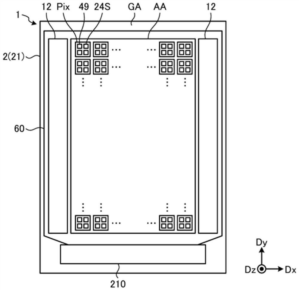
[0025] Modes (embodiments) for carrying out the present invention will be described in detail with reference to the drawings. The present disclosure is not limited to the contents described in the following embodiments. In addition, the constituent elements described below include elements that are easily conceivable by those skilled in the art and substantially the same elements. Furthermore, the constituent elements described below can be appropriately combined. It should be noted that what is disclosed is merely an example, and appropriate changes within the gist of the invention that can be easily conceived by those skilled in the art are naturally included in the scope of the present invention. In addition, in order to clarify the description, the drawings sometimes schematically show the width, thickness, shape, etc. of each part compared with the actual form, but these are just examples and are not intended to limit the interpretation of the present invention. In addi...


PUM


Abstract

The invention provides an inspection method of an array substrate, a display device and an inspection jig, which can well inspect the characteristics of an array substrate on which light-emitting elements are not mounted. The inspection method of an array substrate comprises the following steps: preparing an array substrate on which a plurality of light-emitting elements are not mounted; using an inspection jig including a first connection terminal, a second connection terminal, and an inspection capacitor provided between the first connection terminal and the second connection terminal, connecting the first connection terminal to a mounting electrode, and connecting the second connection terminal to a pixel cathode electrode; and supplying an inspection signal to a transistor on the basis of a control signal from an inspection control circuit that controls inspection of the array substrate, and detecting an output signal output from the transistor in accordance with the inspection signal.

Description

technical field [0001] The invention relates to an inspection method of an array substrate, a display device and an inspection fixture. Background technique [0002] A display device using a micro-sized light-emitting diode (micro LED (micro LED)) as a display element is attracting attention (for example, refer to Patent Documents 1 and 2). Display devices using light emitting diodes are difficult to manufacture such as mounting the light emitting diodes on a substrate due to the small size of the light emitting diodes, which easily leads to failure of the light emitting diodes. Patent Document 1 describes a method of inspecting a plurality of LEDs formed on a sapphire substrate. In addition, Patent Document 2 describes an inspection method for detecting threshold voltages of pixels in real time. [0003] Patent Document 1: Japanese Patent Laid-Open No. 2019-78685 [0004] Patent Document 2: Specification of US Patent Application Publication No. 2017 / 0103702 [0005] In ...

Claims


Application Information

Patent Timeline
Patent Type & Authority Applications(China)
IPC IPC(8): G09G3/00G09F9/33
CPCG09G3/006G09F9/33
Inventor 池田雅延青木义典小川耀博
Owner JAPAN DISPLAY INC
Features
  • R&D
  • Intellectual Property
  • Life Sciences
  • Materials
  • Tech Scout
  • Unparalleled Data Quality
  • Higher Quality Content
  • 60% Fewer Hallucinations
Learn More