
LED chip and preparation method thereof and preparation method of LED display module

A technology of LED chips and display modules, which is applied in the direction of electrical components, electric solid devices, circuits, etc., can solve the problems of top damage, unsatisfactory, colored lines, etc., and achieve the effect of enhancing the strength of the bottom, realizing the display effect, and increasing the distance

Pending Publication Date: 2022-01-18
UNILUMIN GRP
View PDF0 Cites 0 Cited by
  • Summary
  • Abstract
  • Description
  • Claims
  • Application Information

AI Technical Summary

Problems solved by technology

[0002] Due to the increasing market demand for small screen pitches, indoor small-pitch products have become the main space for technological development in the display field, and as the demand for pitches becomes smaller and smaller, traditional discrete devices cannot meet the limits of existing processes. Realization, that is, traditional devices cannot meet the needs of products below P0.7
At this time, COB (Chip On Board, chip-on-board packaging) products have a place in the small-pitch market because of their low cost, high reliability, high protection, and easy cleaning. However, the ink color consistency of COB products and the brightness between modules Problems such as wires and colored wires have not been well resolved, resulting in the COB full screen effect not as good as traditional SMD products, which affects the market promotion of COB products
When using conventional LED chips, during the die-bonding process, due to the fragile light-emitting layer at the bottom of the chip, top damage often occurs; in order to solve the ink color consistency and improve the contrast, we will spray ink or spray black between the chips. However, due to the capillary phenomenon, the ink or black glue will climb up along the side of the chip while covering the electrode 33. The inconsistent climbing height will lead to inconsistent side light emission, which will affect the side viewing effect of COB products; The optical structure or the optical film on the surface will cause the COB packaging surface to be too thick, resulting in the problem of bright lines and colored lines between modules.

Method used


Image

  • LED chip and preparation method thereof and preparation method of LED display module
  • LED chip and preparation method thereof and preparation method of LED display module
  • LED chip and preparation method thereof and preparation method of LED display module

Examples


Embodiment Construction

[0029] In order to describe the technical content, achieved goals and effects of the present invention in detail, the following descriptions will be made in conjunction with the embodiments and accompanying drawings.

[0030] As mentioned in the background technology, the problem of poor light emitting effect of LED chips in the prior art is found by the inventors to be the most prominent in the field of Mini LED chips (LED chips with a size between 50 and 200 μm). The reason for this problem is that in order to solve the ink color consistency and improve the contrast, it is a common technical means to spray ink or black glue between the chips, but due to the capillary phenomenon, the climbing height of the ink or black glue on the side of the chip is different. The light emitted from the side of the chip will bring adverse effects. Based on this, this application proposes an LED chip and its preparation method and packaging method, which can be applied to the field of convent...


PUM


Abstract

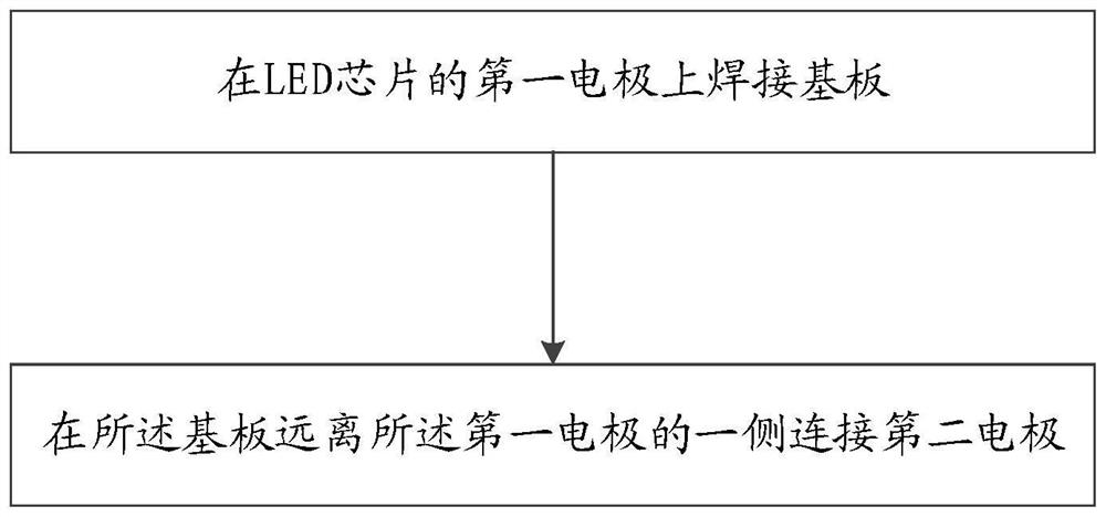
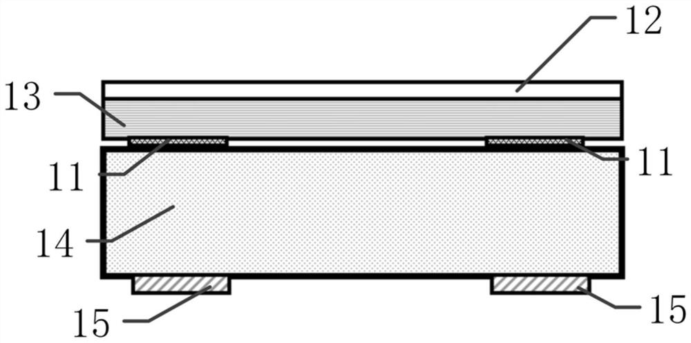
The invention provides a manufacturing process of an LED chip and the LED chip. The LED chip comprises a light-emitting layer, a substrate and an electrode, wherein the substrate is arranged between the light-emitting layer and the electrode, a substrate is welded on the first electrode of an initial LED chip, and a second electrode is connected to one side, far away from the first electrode, of the substrate to obtain the LED chip. According to the invention, the substrate enhances the strength of the bottom of the LED chip, so that the condition that the bottom is damaged by jacking in the process of connecting with the PCB is avoided; the substrate can increase the height of the light-emitting layer on the LED chip to increase the distance between the light-emitting layer and the PCB, so that the operation is easier when a shielding material is used for shielding the exposed part of the PCB substrate subsequently; and when a climbing phenomenon occurs when the shielding material shields the PCB, only the substrate is shielded, and the light-emitting layer is not shielded, so that the display effect of the COB product is improved.

Description

technical field [0001] The invention relates to the field of LEDs, in particular to an LED chip, a preparation method thereof, and a preparation method of an LED display module. Background technique [0002] Due to the increasing market demand for small screen pitches, indoor small-pitch products have become the main space for technological development in the display field, and as the demand for pitches becomes smaller and smaller, traditional discrete devices cannot meet the limits of existing processes. Realization, that is, traditional devices cannot meet the needs of products below P0.7. At this time, COB (Chip On Board, chip-on-board packaging) products have a place in the small-pitch market because of their low cost, high reliability, high protection, and easy cleaning. However, the ink color consistency of COB products and the brightness between modules Problems such as wires and colored wires have not been well resolved, resulting in the COB full-screen effect not a...

Claims


Application Information

Patent Timeline
Patent Type & Authority Applications(China)
IPC IPC(8): H01L25/075H01L33/00H01L33/62
CPCH01L25/0753H01L33/62H01L33/0093
Inventor 张世诚张金刚
Owner UNILUMIN GRP
Learn More