Three-dimensional memory and manufacturing method thereof

A manufacturing method and memory technology, applied in the field of semiconductors, can solve the problems of high difficulty in three-dimensional memory technology, reduced yield and reliability of three-dimensional memory, and achieve the effects of reducing connection length, improving reliability, and simplifying process difficulty

Pending Publication Date: 2022-02-11
YANGTZE MEMORY TECH CO LTD
View PDF0 Cites 0 Cited by
  • Summary
  • Abstract
  • Description
  • Claims
  • Application Information

AI Technical Summary

Problems solved by technology

[0003] As the number of stacked layers of the three-dimensional memory increases, the process of forming the three-dimensional memory becomes more and more difficult, resulting in a decrease in the yield and reliability of the three-dimensional memory. Therefore, it is necessary to continuously optimize the process of forming the three-dimensional memory to continuously improve the device performance Yield and Reliability

Method used


Image

  • Three-dimensional memory and manufacturing method thereof
  • Three-dimensional memory and manufacturing method thereof
  • Three-dimensional memory and manufacturing method thereof

Examples


Embodiment Construction

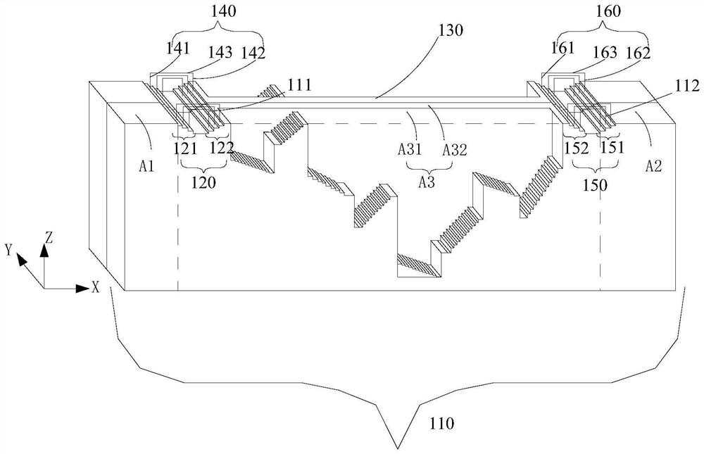
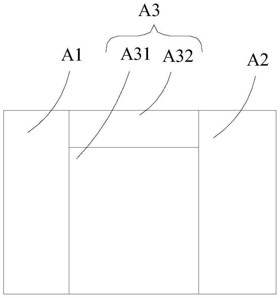
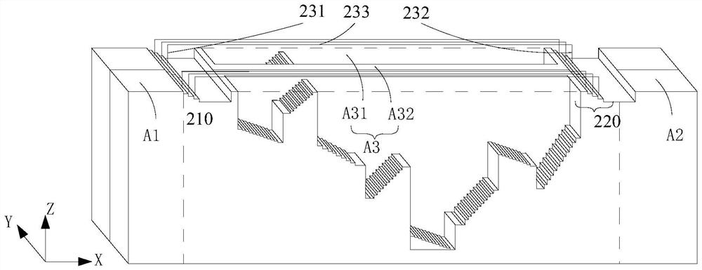
[0031] The present invention will be described in further detail below in conjunction with the accompanying drawings and embodiments. In particular, the following examples are only used to illustrate the present invention, but not to limit the scope of the present invention. Likewise, the following embodiments are only some but not all of the embodiments of the present invention, and all other embodiments obtained by persons of ordinary skill in the art without creative efforts fall within the protection scope of the present invention.

[0032] In addition, the directional terms mentioned in the present invention, such as [top], [bottom], [front], [back], [left], [right], [inside], [outside], [side], etc., only is the direction with reference to the attached drawings. Therefore, the directional terms used are used to illustrate and understand the present invention, but not to limit the present invention. In the various figures, structurally similar elements are denoted by th...


PUM


Abstract

The invention provides a three-dimensional memory and a manufacturing method thereof, and the three-dimensional memory. The three-dimensional memory comprises a substrate; a stacking structure, comprising a first storage area, a step area and a second storage area; a step region, comprising a sub-step region; a partition wall structure; a first top selection step structure, comprising a first main step structure and a first auxiliary step structure which are distributed in the first transverse direction, and the first main step structure and the first auxiliary step structure being provided with first gate layers with the corresponding layer number and height in the longitudinal direction; and first connecting structures, connected with the first gate layers with the corresponding layer number and height in the first main step structures and the first auxiliary step structures. The first gate layers in the first main step structure and the first auxiliary step structure are connected through the first connecting structure, the length of the connecting line of the first connecting structure can be effectively reduced, the resistance value of the connecting line is reduced, meanwhile, the subsequent process difficulty is simplified, and the reliability of the device is improved.

Description

【Technical field】 [0001] The invention relates to the technical field of semiconductors, in particular to a three-dimensional memory and a manufacturing method thereof. 【Background technique】 [0002] Three-dimensional memory (3D NAND Flash) is widely used in computers, solid-state hard disks and electronic devices due to its high storage density and fast programming speed. Three-dimensional memory can achieve higher data storage density by adopting vertical device technology. Alternately stacked multi-layer data storage units are formed in the three-dimensional memory, and the planar structure is transformed into a three-dimensional structure to improve the storage density and integration of the three-dimensional memory. Three-dimensional memory enables higher storage capacity in less space, resulting in significant cost savings, reduced power consumption, and dramatic performance gains for many consumer mobile devices and the most demanding enterprises Deployment needs. ...

Claims


Application Information

Patent Timeline
Patent Type & Authority Applications(China)
IPC IPC(8): H01L27/11582H01L27/1157H01L27/11575H01L27/11556H01L27/11524H01L27/11548H10B43/27H10B41/27H10B41/35H10B41/50H10B43/35H10B43/50
CPCH10B41/35H10B41/50H10B41/27H10B43/35H10B43/50H10B43/27
Inventor 孔翠翠张中周文犀
Owner YANGTZE MEMORY TECH CO LTD
Why Eureka
Try Eureka