Display device and manufacturing method thereof

A technology of display device and manufacturing method, which is applied in the direction of electric solid device, semiconductor device, electrical components, etc., can solve the problems of increasing the surface height difference of the display device and affecting the QLED packaging effect, and achieve the effect of improving the packaging effect.

Pending Publication Date: 2022-02-11
GUANGDONG JUHUA PRINTING DISPLAY TECH CO LTD +2
View PDF0 Cites 0 Cited by
  • Summary
  • Abstract
  • Description
  • Claims
  • Application Information

AI Technical Summary

Problems solved by technology

[0006] Based on this, it is necessary to provide a display device and its manufacturing method to solve the problem that the surface height difference of the display device is significantly increased due to the thickness of the Micro-LED being much larger than that of the QLED, which affects the encapsulation effect of the subsequent QLED.

Method used


Image

  • Display device and manufacturing method thereof
  • Display device and manufacturing method thereof
  • Display device and manufacturing method thereof

Examples


Embodiment 1

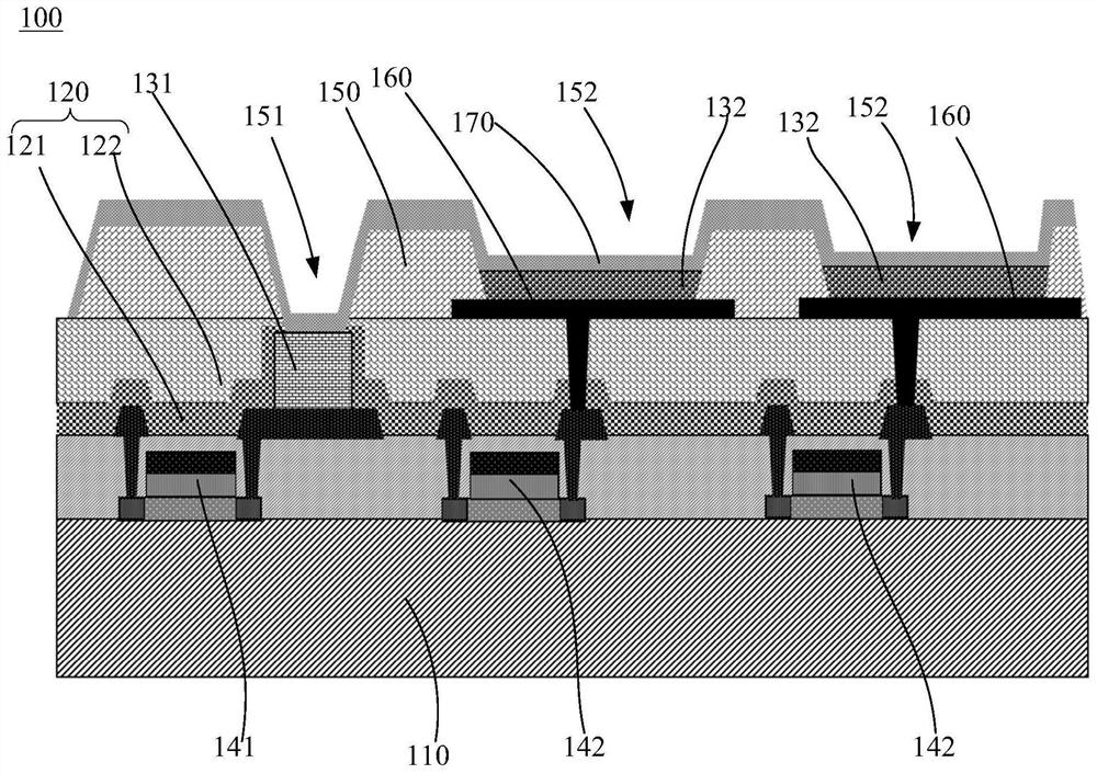
[0083] This embodiment provides a display device 100 .

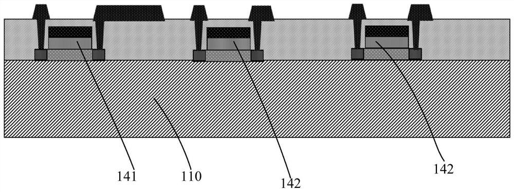
[0084] Please refer to figure 1 As shown, the display device 100 of this embodiment includes a substrate 110 , a first driving TFT 141 , a second driving TFT 142 , a passivation layer 121 , a flat layer 122 , a pixel defining layer 150 , a first sub-pixel 131 and a second sub-pixel 132 .

[0085] The first driving TFT 141 and the second driving TFT 142 are arranged in an array on the substrate 110 .

[0086] The first sub-pixel 131 is a blue Micro-LED chip with a vertical structure. The first sub-pixel 131 is arranged on the source of the second driving TFT 142. The surface of the first sub-pixel 131 near the substrate 110 is completely connected to the first driving TFT 141 source contact.

[0087]The passivation layer 121 covers the first driving TFT 141 and the second driving TFT 142 . The planarization layer 122 covers the passivation layer 121 . The first sub-pixel 131 is buried in the intermediate layer 120 com...

Embodiment 2

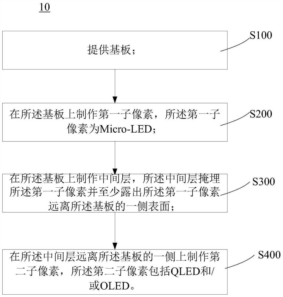
[0091] This embodiment provides a manufacturing method of the display device 100 . In this embodiment, some conventional processes for manufacturing the display device 100 may be omitted between steps and between specific steps before and after operations, and those skilled in the art may add process steps according to actual needs during the manufacturing process.

[0092] Please refer to Figure 3 to Figure 8 As shown, the manufacturing method of the display device 100 of this embodiment includes the following steps:

[0093] Step 1, providing a substrate 110 .

[0094] Step 2, such as image 3 As shown, the first driving TFT 141 and the second driving TFT 142 are fabricated on the substrate 110 , wherein the source surface area of ​​the first driving TFT 141 is larger.

[0095] Step 3, such as Figure 4 As shown, the first sub-pixel 131 is transferred to the source of the first driving TFT 141 by a transfer process, and the first sub-pixel 131 is a blue Micro-LED chip w...


PUM


Abstract

The invention relates to a display device. The display device comprises a substrate, a middle layer, a first sub-pixel and a second sub-pixel, the intermediate layer covers the substrate. The first sub-pixel is a Micro-LED, and the second sub-pixel comprises a QLED and / or an OLED. The first sub-pixel is embedded in the middle layer, and the middle layer at least exposes the surface of the sides, away from the substrate, of the first sub-pixel. The second sub-pixel is disposed on a side of the intermediate layer away from the substrate. According to the display device and the manufacturing method thereof, the first sub-pixel and the second sub-pixel are arranged on the substrate, the middle layer is arranged on the substrate, the first sub-pixel is embedded in the middle layer, the middle layer at least exposes the surface of the side, away from the substrate, of the first sub-pixel, and the second sub-pixel is arranged on the side, away from the substrate, of the middle layer; therefore, the first sub-pixels are closer to the substrate than the second sub-pixels, so that the situation that the first sub-pixels are too high relative to the second sub-pixels can be avoided, and the subsequent packaging effect can be improved.

Description

technical field [0001] The invention relates to the field of display technology, in particular to a display device and a manufacturing method thereof. Background technique [0002] In the contemporary information society, the importance of display devices as a visual information transmission medium is further strengthened. Currently, display devices are developing towards lighter, thinner, lower power consumption, lower cost and better image quality. [0003] Quantum dot light-emitting diodes (QLEDs) have become one of the main research directions of display devices due to their advantages such as self-luminescence, fast response, wide viewing angle, high brightness, and thinness. At present, both red and green QLEDs are close to commercial requirements in terms of efficiency and lifespan, but blue QLEDs are still lacking in efficiency and lifespan, and their progress is relatively slow, which affects the progress of mass production of full-color QLEDs. Likewise, blue OLED...

Claims


Application Information

Patent Timeline
Patent Type & Authority Applications(China)
IPC IPC(8): H01L27/32H01L27/15
CPCH01L27/15H10K59/122H10K59/123H10K59/124H10K59/1213H10K59/126
Inventor 陈亚文史文付东
Owner GUANGDONG JUHUA PRINTING DISPLAY TECH CO LTD
Why Eureka
Try Eureka